
Introduction
The integration of multiple digital signal processing (DSP) blocks, wideband digital-to-analogue converters (DACs), and wideband analogue-to-digital converters (ADCs) within a single monolithic chip is now enabling the offload of power hungry FPGA resources to allow for smaller footprint, lower power, increased channel count platforms that can sample at higher rates than previously achievable. Along with this new capability comes novel multichip synchronisation (MCS) algorithms within these integrated circuits (ICs), which allow users to achieve a known (deterministic) phase for all channels when powering the system or otherwise making software modifications to the system. This deterministic phase therefore simplifies the broader system-level calibration algorithms needed to achieve the synchronisation of all channels at the output or input to the front-end networks attached to these ICs. This article presents experimental results that demonstrate this MCS capability while using a 16-channel receiver/transmitter platform consisting of multiple digitiser ICs, clock sources, and digital interfaces.
High Level System Block Diagram
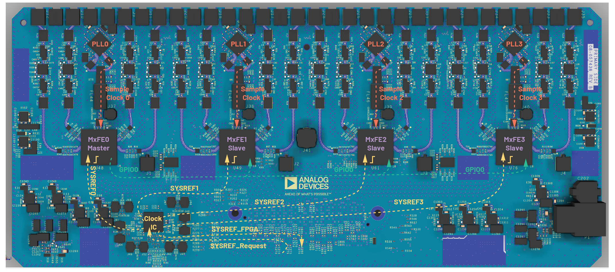
A block diagram of the system used for this test is shown in Figure 1 and consists of four integrated DAC/ADC/DSP ICs that each consist of four 12GSPS DACs, four 4GSPS ADCs, and 12 digital up-converter (DUC) and 12 digital down-converter (DDC) blocks. The DUCs/DDCs allow frequency translation and/or interpolation/decimation within the digital domain. Using a single 500MHz reference clock injected onto the board, a reference-locked clock buffer is then utilised to generate the system reference signals needed for MCS as well as the clocks required for the digital interface to the baseband processor (BBP). The system also contains four separate phase-locked loop (PLL) synthesisers that generate the 12GHz sources needed to clock each digitising IC from the common reference. An RF front end is attached to each digitiser output/input, which creates a filtered and amplified signal to/from the edge-launched RF connectors. A full power distribution solution is implemented. All voltages required for the system are generated from a single 12V source. All transmit signals propagate on the bottom of the board, whereas all receive signals propagate on the top of the board to achieve the most optimum channel-to-channel isolation.
Subarray Clock Tree Structure
As previously mentioned, the subarray clock tree consists of a single 500MHz reference source that is split and sent to the reference inputs of four separate PLL synthesiser ICs, as shown in Figure 1. This 500MHz signal is also 10dB coupled, amplified, and sent into another clock buffer IC that is responsible for generating the system references (SYSREFs) and BBP clocks required for the digital interface. The goal of this clock tree is threefold, as it:
The clock tree ICs are chosen to demonstrate that various board layout anomalies can be corrected in software and/or hardware with the help of digital and analogue delay blocks present within these chips. Ultimately the result is a clock tree that can provide a SYSREF pulse to all required ICs within the same sample clock cycle of each of these ICs.
Digital Interface with Baseband Processor
The four digitising ICs each establish a JESD204B or JESD204C digital link interface with the BBP.1,2 This interface is responsible for transmitting the ADC and DAC codes over the physical traces (SERDES) to and from the BBP. The number of differential SERDES traces used in this interface is termed the number of lanes (L) for this link. The converter bit resolution sent over the link is regarded as N'. The number of channelised data paths, also coined virtual converters, is labelled as M. The results shown in this article use a JESD204C link with M = 16, N' = 16, L = 4 for the DAC-side links and M = 8, N' = 16, L = 2 for the ADC-side links.
The rate at which data is transmitted and received between the digitiser IC and the BBP is coined the lane rate. The DSP blocks on silicon (that is, the DDCs/DUCs) allow the user to sample the digitisers at a different rate than the data rate sent across the physical lanes. As such, the lane rate is dependent on the digitally decimated/interpolated data rate for each data path. For this work, a 250 MSPS I/Q data rate has been utilised. For a JESD204C interface, the lane rate is defined as:
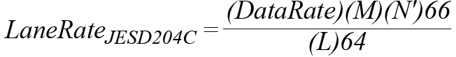
whereas for a JESD204B interface, the lane rate is defined as:
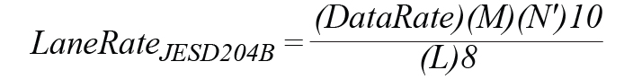
The results shown in this article use a lane rate of 16.5Gbps for both the ADC- and the DAC-side JESD204C links.
Each JESD204B/JESD204C link can be established within different subclasses. These subclasses are separated based on whether multichip synchronisation or deterministic latency is required. For this work, the data shown uses a JESD204C Subclass 1 mode, and therefore utilises SYSREF signals to align portions of the digital data transmitted across the multiple links present within the system. Specifically, in this JESD204C Subclass 1 mode, the SYSREF signals are used to align the local extended multiblock counter (LEMC), which transmits at a rate:
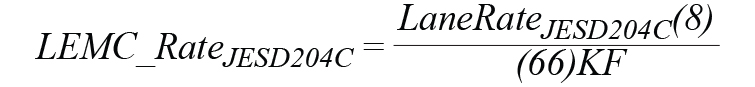
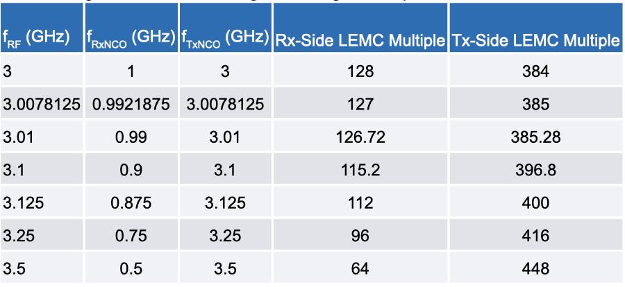
where F is the number of octets per JESD frame per lane and K is the number of frames per single multiframe. For this work, F = 8 and K = 32, and therefore an LEMC rate of 7.8125MSPS is used. Knowledge of this LEMC rate is important, as any successful MCS routine will need to demonstrate that RF frequencies that are not an integer multiple of the LEMC rate are able to achieve deterministic power-up phase.
Multichip Synchronisation Method
Within this system, the wideband integrated ADC/DAC ICs provide MCS circuitry to allow power-up deterministic phase on all transmit and receive RF channels, even while using the DUC/DDC DSP blocks within the IC. This MCS feature enables users to populate a lookup table (LUT) during a factory calibration to minimise operational downtime. Any successful MCS demonstration must be capable of providing deterministic phase across all channels within the system for every attempted RF frequency, thermal gradient, and system power cycle.
The integrated ADC/DAC ICs contain 12 DUC blocks and 12 DDC blocks, as shown in Figure 1. Each of these blocks contains an interpolation (DUC) or decimation (DDC) subblock to change the data rate of the DAC digital input signal or ADC digitised output signal, respectively. Also contained within each DUC/DDC is a complex numerically controlled oscillator (NCO), which allows frequency translation within the digital domain. Each of these NCOs is capable of real-time complex phase adjustment such that the digital signal between the DAC/ADC and the BBP can be modified to compensate for various SERDES trace length mismatches.
The MCS feature for these ADC/DAC ICs is responsible for achieving phase determinism throughout all aspects of the digitiser IC’s data path. The workflow to achieve MCS is shown in Figure 2.
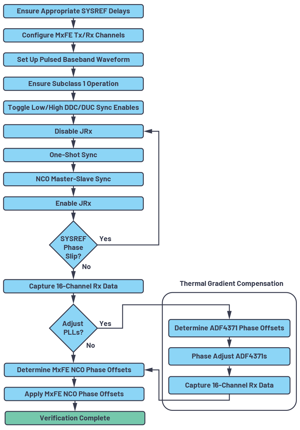
The MCS algorithm can be divided into two separate functions:
The one-shot sync feature first requires that the user defines the JESD link parameters (such as M, N', L, etc.) and then configures the synchronisation logic for any desired SYSREF averaging (if using continuous SYSREF pulses). Additionally, desired LEMC delays can be used to force the LEMC to be generated at a certain delay after the SYSREF edge. After this is completed, the user then enables the one-shot sync bit within each digitiser IC and then requests that SYSREF pulses be sent to each IC within the same clock cycle, as shown in Figure 3. For this system, analogue fine delays have been introduced within the clock buffer IC to allow synchronous SYSREFs to all digitiser ICs. A subsequent check can be executed to verify the one-shot sync process performed successfully by querying registers within each IC that provide information about the phase relationship between the SYSREF signal and the LEMC boundary of each IC’s link. Once a stable phase is measured (that is, once the SYSREF-LEMC phase register reads 0), the user then knows that the LEMCs of all the digitiser ICs are aligned and the user can then proceed to the NCO master-slave sync process. For this activity, the subtasks described for the one-shot sync are contained within an application programming interface (API) provided by the chip manufacturer.
The NCO master-slave sync feature first assigns one of the digitiser ICs within the subarray to act as a master chip, as shown in Figure 3. All other digitisers are then deemed slave ICs. The master IC is set up such that the GPIO0 pin of this device is configured as an output and routed to the GPIO0 nets of the three slave digitiser ICs. The slave GPIO0 nets are configured as inputs. The user can then choose to trigger on either the SYSREF pulse, the LEMC rising edge, or the LEMC falling edge. For the data shown in this article, the LEMC rising edge is used as the NCO master-slave sync trigger source and the GPIO nets are routed through the BBP instead of locally on the subarray. Next, the DDC synchronisation bits are toggled low and then high to arm the ADC-side NCO synchronisation algorithm. Likewise, the microprocessor align bit is toggled low and then high to arm the DAC-side NCO synchronisation algorithm.
When this trigger is requested, at the next LEMC rising edge the master digitiser IC asserts high a master out signal through its GPIO0 net. This signal propagates to the GPIO0 inputs of each of the slave devices. At the next LEMC edge, all digitiser ICs experience an NCO reset algorithm. After this, any LEMC pulses are ignored with regards to the NCO master-slave sync algorithm. As with the one-shot sync, these NCO master-slave sync subtasks are contained within API functions for user ease of use.
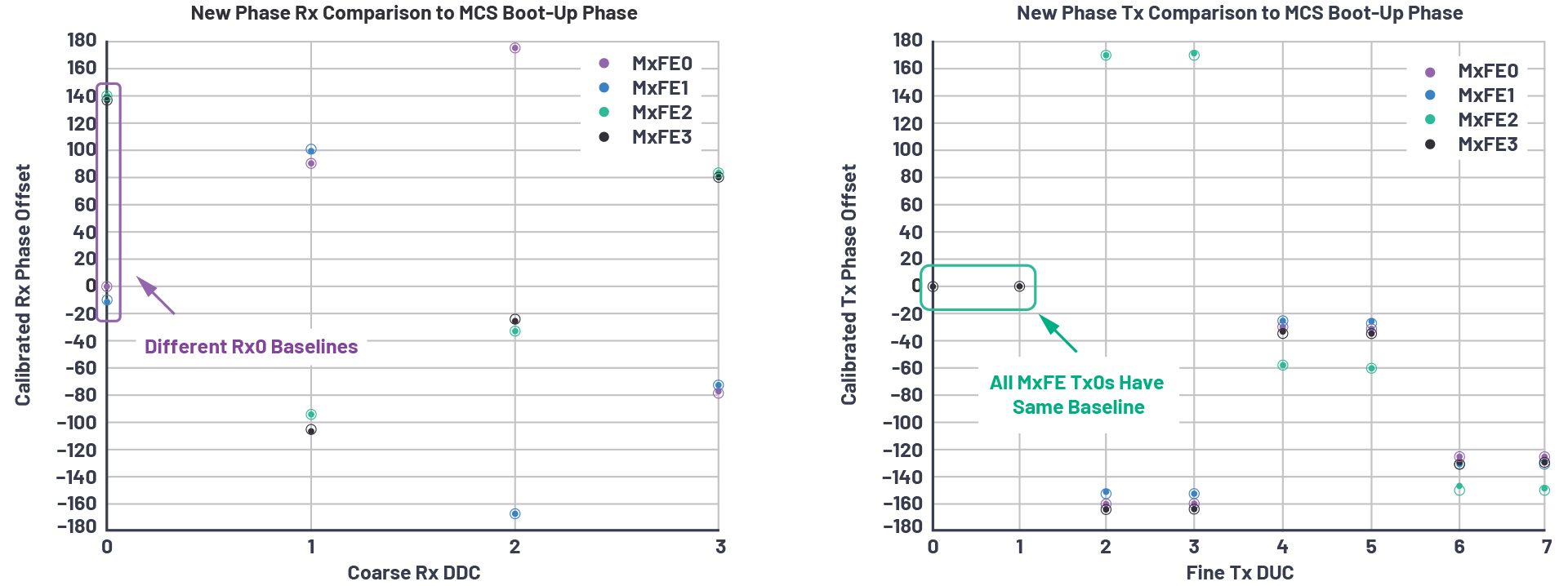
Using both the one-shot sync and the NCO master-slave sync features aligns both inputs to every DDC/DUC such that the output phase offset of each receive and transmit channel is repeatable after multiple power cycles, as shown in Figure 4. The data in Figure 4 shows the calibrated phase offsets over 100 power cycles (indicated by multiple solid dots) for each receive and transmit channeliser while the system is operating under a static thermal gradient during each reboot.
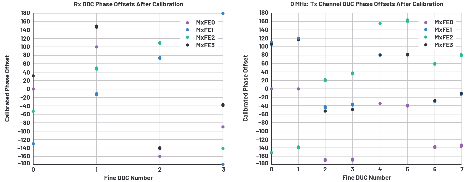
As can be seen from the multiple dots present in this figure, the dots of each colour for a given DDC/DUC are all tightly clustered to the same position after power cycles, thereby portraying deterministic phase for that particular channel. For the data in this test, all eight channeliser DUCs have been used on the transmit side, whereas only four of the eight channeliser DDCs are used. However, it has been confirmed that indeed all eight channeliser DDCs provide deterministic phase while using the MCS algorithm as well.
Issuing this algorithm at boot-up establishes a deterministic phase for each channel if the PLL synthesiser sample clocks and clock IC SYSREFs maintain the same phase relationship at boot-up. However, any system will undergo thermal gradients, which can result in PLL clock drift, and which can result in a different power-up phase if left uncompensated. To compensate for thermal gradient drift within the system, this platform utilises PLL synthesiser phase adjustments.
PLL Synthesiser Phase Adjustments
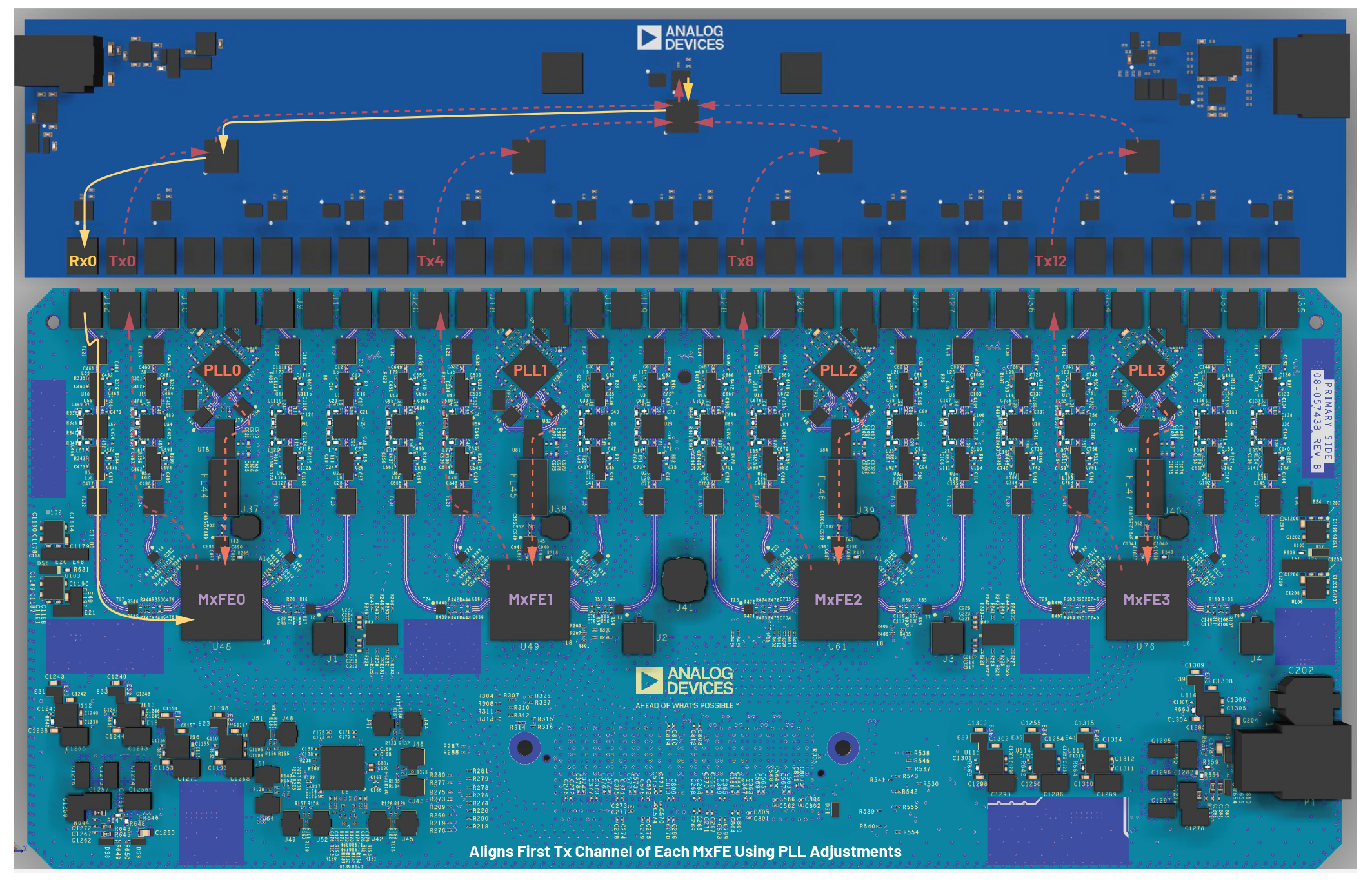
The chosen PLL synthesiser ICs have been selected to allow for relative sample clock phase adjustments injected into each digitiser IC. Thermal drift, and the resulting PLL phase drift between the sample clock and the SYSREF of each IC, is compensated by creating a feedback mechanism that ensures that the first transmit channel of each digitiser IC is phase aligned to the first digitiser IC’s first transmit channel. To achieve this feedback loop, the first transmit channel of each IC outputs a signal that differentiates itself from the other transmit channels, as shown in Figure 5. These four signals are combined and sent into a common receiver, which for this system is labelled Rx0.
Simultaneous receive data is obtained for all receive channels, which then allows users to apply cross-correlation techniques and determine the complex phase offsets between these four transmit channels, ΦTxOffset. The PLL synthesiser ICs contain within them a voltage controlled oscillator (VCO) that is operating at a frequency ƒVCO_PLL.
The measured phase offsets ΦTxOffset are then related to the required PLL phase adjustment ΦPLL_Adj and the RF frequency ƒ carrier such that:
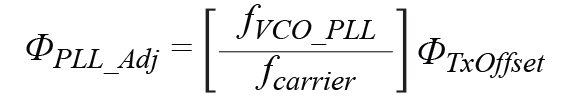
Using this formula, the PLL synthesiser phases can be adjusted by a new known amount to establish a common transmit baseline between all digitiser ICs for all power cycles, as shown in Figure 6. The open circles for each channel shown in Figure 6 correspond to the first power cycle, whereas all the other solid dots correspond to subsequent power cycles. As can be seen from this figure, the calibrated transmit phase offsets for the first (and second) channelisers of all digitiser ICs are phase aligned. The second channeliser of each digitiser IC is aligned in this instance as well, because two channelisers are used for each DAC in the system.
Adding this PLL synthesiser phase adjustment step prior to the MCS routines discussed in the earlier section thereby creates a deterministic phase across all induced thermal gradients within the system by forcing the system to the same sample clock-SYSREF phase relationship, which is manifested as a transmit alignment baseline across all digitiser ICs. Figure 7 shows that an induced thermal gradient can be detected via the temperature measurement unit (TMU) on each PLL synthesiser chip. As can be seen from the blue trace in the bottom left of Figure 7, widely varying temperatures across the platform have been intentionally induced by applying different fan airflows to the system. Using the PLL phase adjustment for each IC, however, demonstrates that regardless of the airflow applied to the board, the calibrated NCO phase offsets for each receive and transmit channel are deterministic when forcing the first transmit channeliser of each digitiser IC to be aligned to each other. This is revealed by observing the tight cluster of the same colour of dots on the top two plots in Figure 7 despite the different thermal gradients applied to the board during different power cycles.
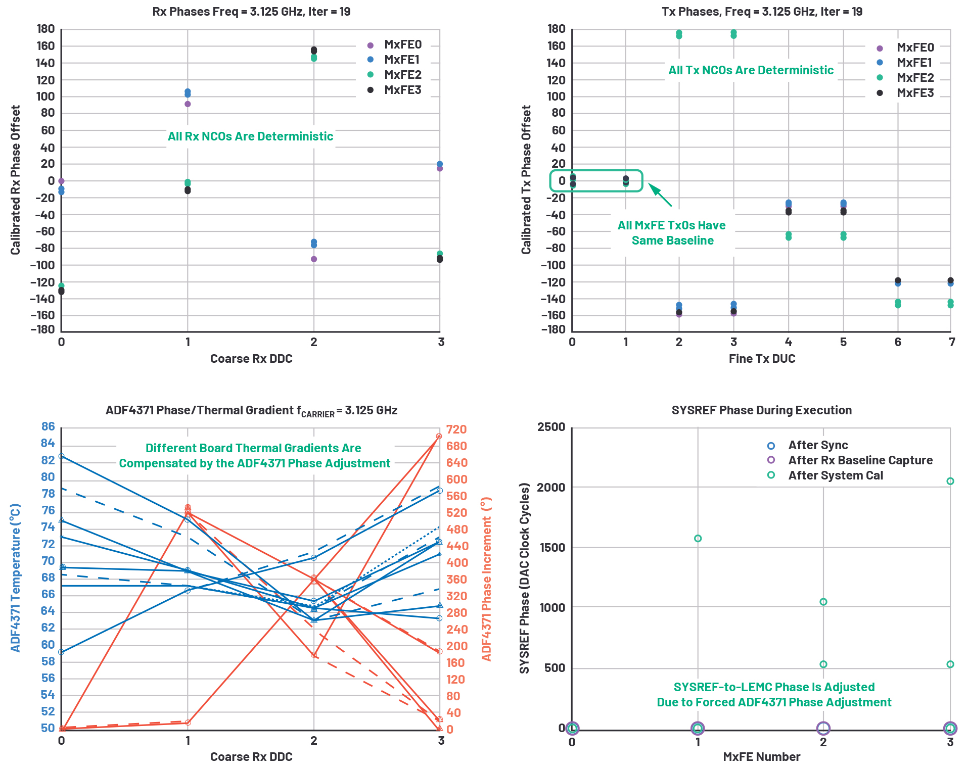
Shown on the bottom right of Figure 7 is the polled digitiser IC registers, which show the measured SYSREF-LEMC phase relationship after applying the PLL synthesiser phase offset. Note from the orange traces on the bottom-left plot that the PLL synthesiser phase adjustments fully compensate any measured non-zero SYSREF phases resulting from a different induced thermal gradient.
Many frequencies have been measured, all of which demonstrate deterministic receive and transmit phase. The specific frequencies chosen for this article are shown in Figure 8, and were chosen such that MCS is demonstrated over many induced thermal gradients when using non-integer multiples of the reference clock or the LEMC.
Scalability to Multiple Subarrays
The data shown in this article is primarily focused on MCS performance at the subarray level, but there is also a need to ensure that these synchronisation features are realisable at the larger array level and across multiple subarrays. To achieve this higher level of synchronisation, an array-level clock tree is required to ensure that the SYSREF requests to each subarray shown in Figure 1 synchronously arrive at each subarray’s clock buffer IC. Then, given this criterion, each subarray can issue the required SYSREFs and BBP clocks as described earlier such that these signals arrive at the subarray digitiser ICs and BBP within the same sample clock cycle across the larger array. This array-level clock tree requires that the clock distribution to each subarray possesses the delay adjustment blocks necessary to achieve synchronous SYSREF request distribution to each of the downstream subarray clock chip ICs. In this manner, multiple BBPs connected to multiple subarrays are ultimately synchronised.
System-Level Calibration Algorithm
While the MCS algorithms shown in previous sections do provide power-up deterministic phase for each receive and transmit channel, these phases are not necessarily phase-aligned across all channels within the RF domain due to any differences in RF front-end trace lengths across channels. Therefore, while the MCS algorithms do indeed simplify the array calibration process, there is still a need to undergo a system-level calibration routine to align the phases of each RF channel within the system.
It is therefore necessary to develop an efficient system-level calibration algorithm in addition to performing the MCS algorithms. The system-level calibration method for this article utilises a specific baseband waveform and is completely self-contained without the need for any external equipment. The system described in this article is capable of injecting separate baseband waveforms into each channeliser on the platform. Utilising this capability, a baseband waveform consisting of a one-period pulse for each transmit channeliser is injected in the subarray, as shown in the bottom-left of Figure 9. Each transmit channelisertherefore outputs only one pulse. However, the waveforms are staggered across all transmit channelisers such that only one one-period pulse is output at a time throughout the system. The output of all transmit channelisers is combined within the RF domain and then split and sent back into all receive channels, as shown in the top of Figure 9. Finally, a simultaneous receive data capture is performed for all receive channels and the data is saved to a 4096x16 matrix, where 4096 is the sample size collected for all 16 receive channels.
This data is then analysed vertically along the first column (corresponding to Rx0) to locate the Tx0 channeliser pulse, as is shown in the top subplot on the bottom-right of Figure 9. After the Tx0 pulse is identified all other pulse locations are known and the complex phase of each pulse’s rising edge is calculated and saved to a 1x16 vector that corresponds to the measured phase offsets present at all transmit channels throughout the system. With this knowledge, and using Tx0 as the baseline reference, the complex phases of all transmit channels are then modified based on the measured offsets.
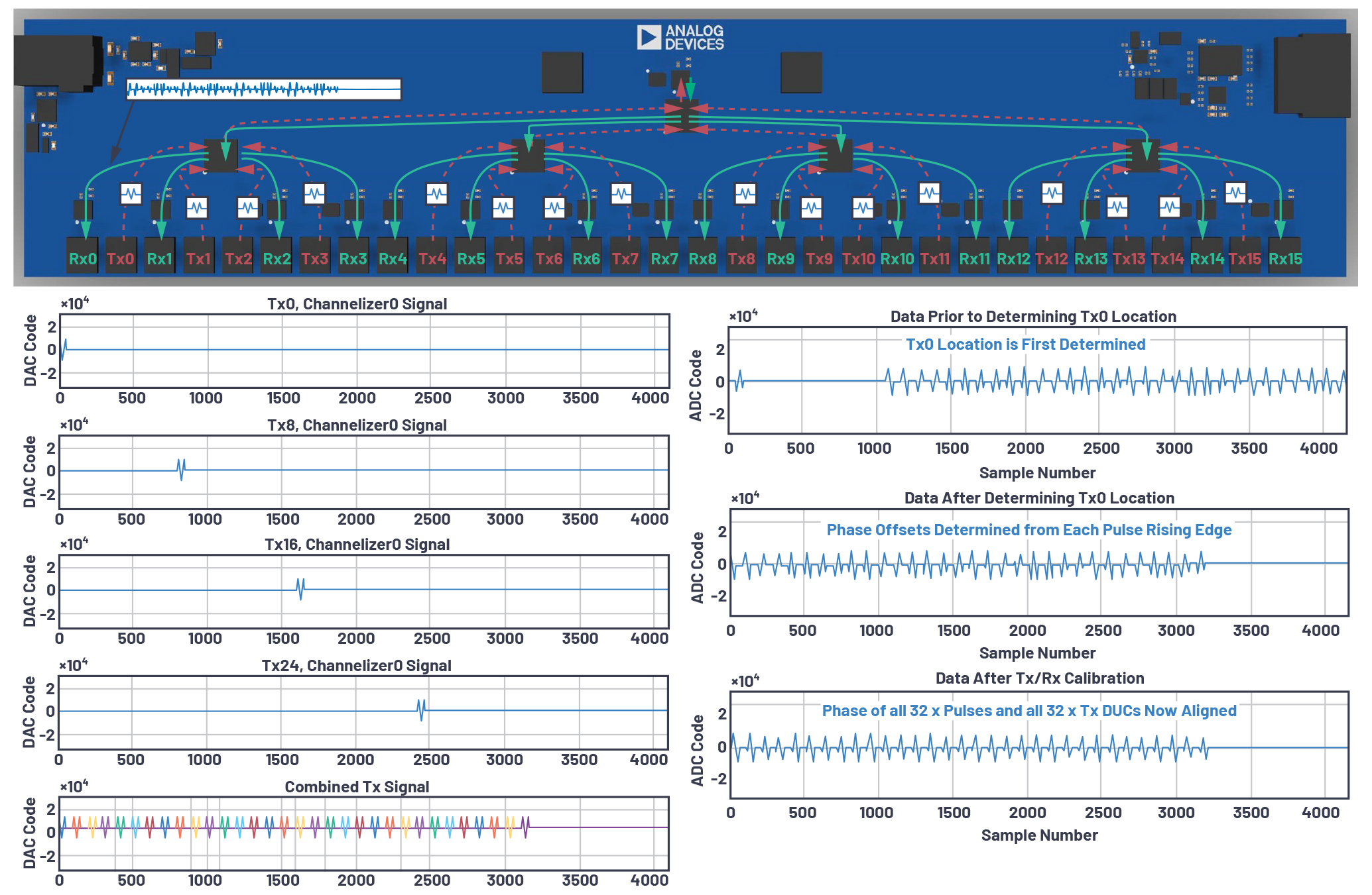
Similarly, since the same combined signal is being sent into all receive channels, the data is then analysed horizontally along the matrix (looking across all receive channels). The complex phases of all receive channels are then measured with respect to Rx0 and saved to a 1x16 vector corresponding to the measured receive phase offsets present in the system. The receive NCO complex phases are then adjusted throughout the subarray to phase align all channels with respect to Rx0, as is shown by the in-phase (I) and quadrature-phase (Q) ADC codes for all 16 receive channels in Figure 10. It may be noticed that, while the plot in Figure 10 phase aligns all channels, it does not necessarily amplitude align all channels. However, using the on-chip finite impulse response (FIR) filters now present on these digitiser ICs, one could alternatively achieve amplitude and phase alignment across channels without the need to allocate power hungry FPGA resources to achieve the same result.
This system-level calibration algorithm is presently achieved in MATLAB® and takes approximately three seconds to complete. However, if implemented in hardware description language (HDL), this calibration time may be further reduced while maintaining a completely self-contained algorithm. Additionally, by relying on the MCS algorithms, if the system frequency and amplitude is known at boot-up, users can load phase offset values from a lookup table instead of needing to undergo the measurements described in this system-level calibration method. In this case, the system-level calibration method can be used to populate the phase offsets saved to a lookup table during a factory calibration.
Conclusion
A successful MCS process has been demonstrated using four Analog Devices’ AD9081 MxFETM ICs as the backbone of the subarray. Thermal gradients across the platform are compensated with the aid of phase adjust blocks within four ADF4371PLL synthesisers. An HMC7043 clock IC is used to distribute the SYSREFs and BBP clocks required for the JESD204C interface. MCS algorithms within the AD9081 allow for simplified system-level calibrations and provide power-up deterministic phase for multiple frequencies and thermal gradients present in the system. An efficient system-level calibration algorithm is also presented that is used to populate LUTs during factory calibration, and therefore dramatically reducessystem boot time. This platform is shown in Figure 11 and is called the Quad-MxFE. The system is available for purchase from Analog Devices. This work is pertinent to any multichannel system present in any phased array radar, electronic warfare, instrumentation, or 5G platform.
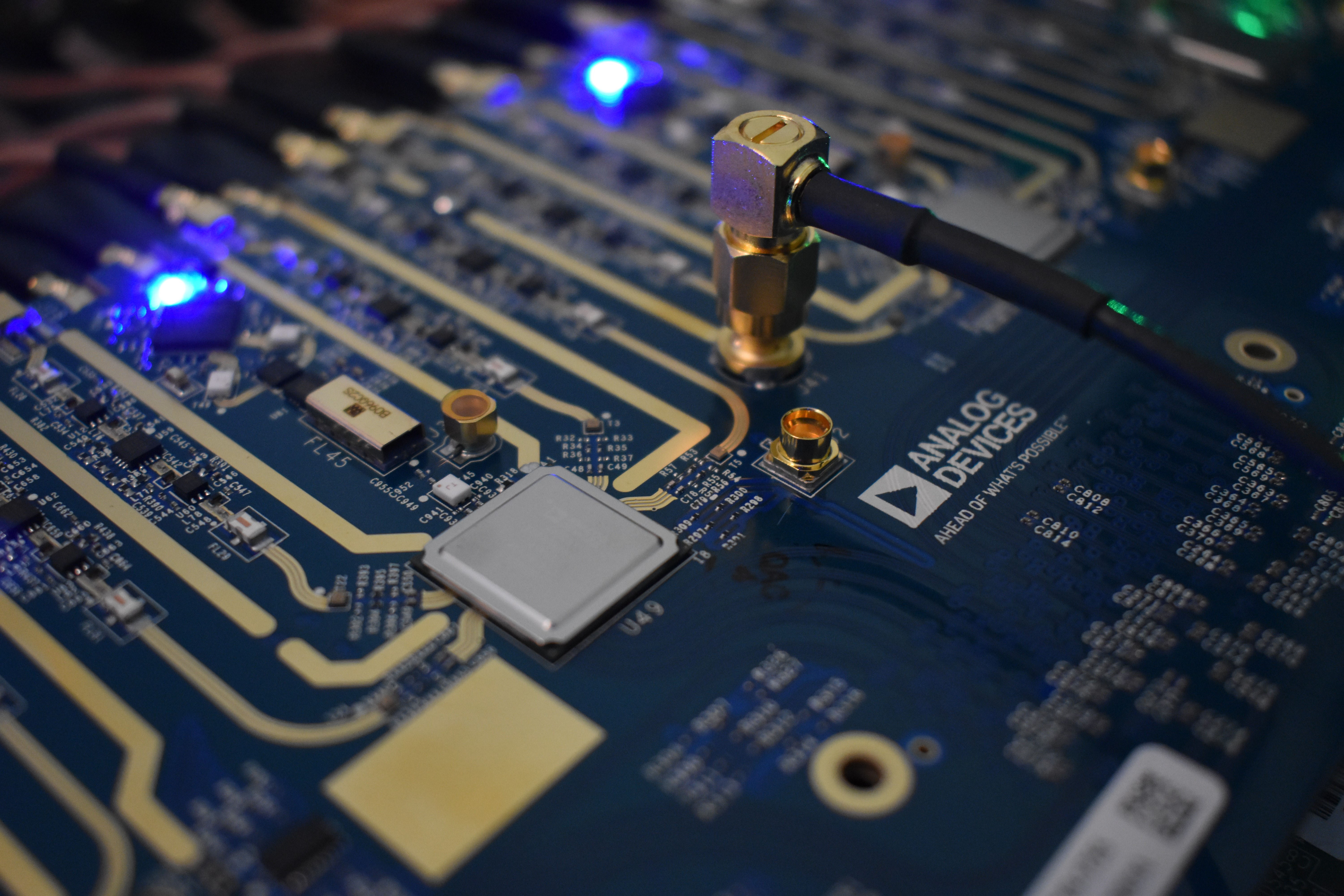
Figure 11. The Quad-MxFE platform is available for purchase from Analog Devices.
References
1 Del Jones. “JESD204C Primer: What’s New and in It for You—Part 1.” Analog Dialogue, Vol. 53, No. 2, June 2019.
2 Del Jones. “JESD204C Primer: What’s New and in It for You—Part 2.” Analog Dialogue, Vol. 53, No. 3, July 2019.
About the Authors
Mike Jones is a principal electrical design engineer with Analog Devices working in the Aerospace and Defense Business Unit in Greensboro, North Carolina. He joined Analog Devices in 2016. From 2007 until 2016 he worked at General Electric in Wilmington, North Carolina, as a microwave photonics design engineer, where he focused on microwave and optical solutions for the nuclear industry. He received his B.S.E.E. and B.S.C.P.E. from North Carolina State University in 2004 and his M.S.E.E. from North Carolina State University in 2006. He can be reached at michael.jones@analog.com.
Michael Hennerich joined Analog Devices in 2004. As a systems and applications design engineer, he has worked on a variety of DSP/FPGA- and embedded processor-based applications and reference designs. Michael now works for the System Development Group (SDG) as an open-source system engineering manager in Munich, Germany. In this role, he is leading ADI’s device driver and kernel development team, developing device drivers for all sorts of mixed-signal IC products and HDL interface cores. He holds an M.Sc. degree in computer engineering and a Dipl.-Ing. (FH) degree in electronics and information technologies from Reutlingen University. He can be reached at michael.hennerich@analog.com.
Peter Delos is a technical lead in the Aerospace and Defense Group at Analog Devices in Greensboro, North Carolina. He received his B.S.E.E. from Virginia Tech in 1990 and M.S.E.E. from NJIT in 2004. Peter has over 25 years of industry experience. Most of his career has been spent designing advanced RF/analogue systems at the architecture level, PWB level, and IC level. He is currently focused on miniaturizing high performance receiver, waveform generator, and synthesiser designs for phased array applications. He can be reached at peter.delos@analog.com.


McMurtry Spéirling defies gravity using fan downforce
Ground effect fans were banned from competitive motorsport from the end of the 1978 season following the introduction of Gordon Murray's Brabham...