
Introduction
In Part 1, we introduced the phased array concept, beam steering and array gain. In Part 2, we presented the concept of grating lobes and beam squint. In this section, we begin with a discussion of antenna sidelobes and the effect of tapering across an array. Tapering is simply the manipulation of the amplitude contribution of an individual element to the overall antenna response.
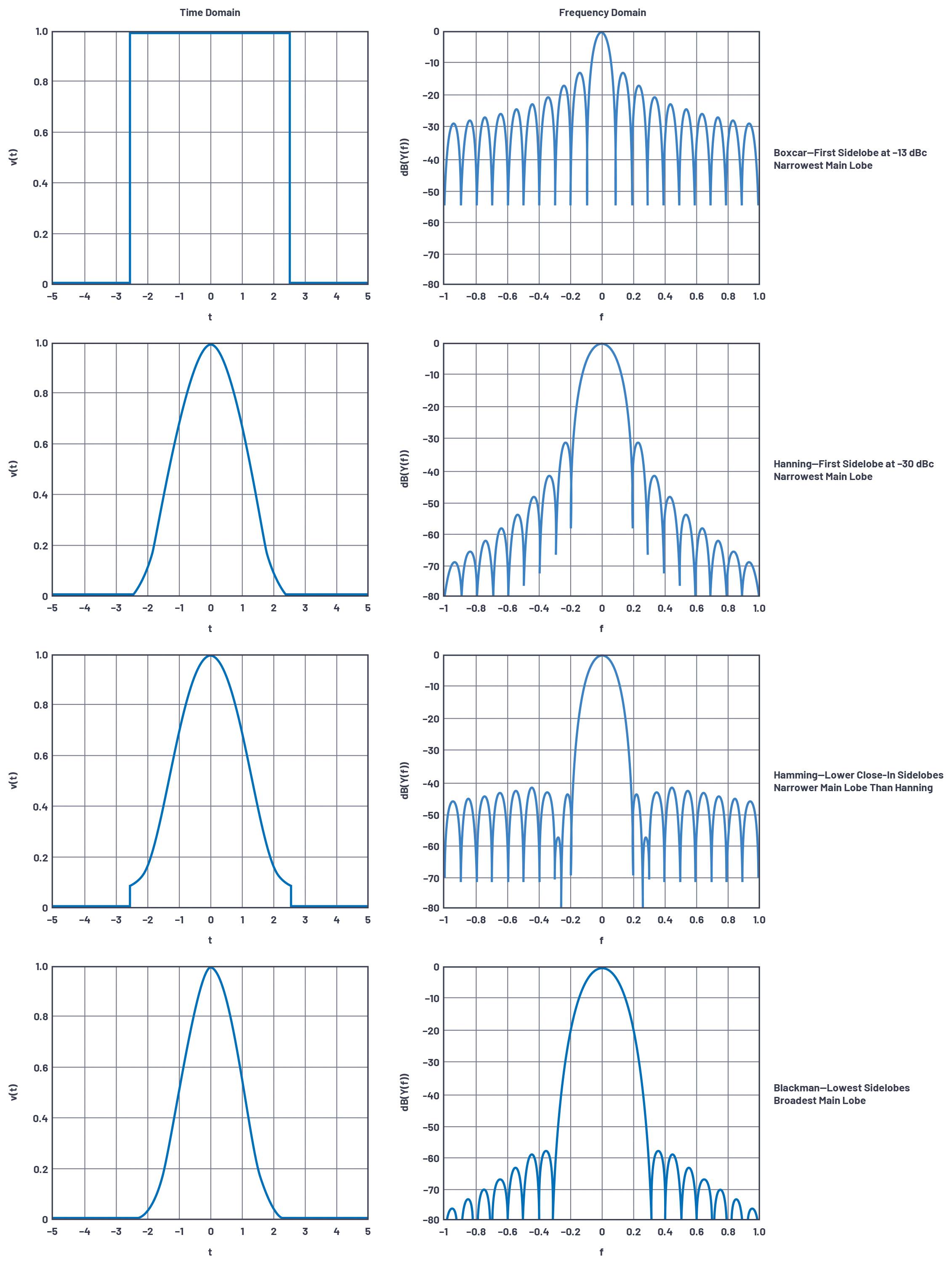
In Part 1, no tapering was applied and the first sidelobes were –13dBc as seen in the figures. Tapering provides a method to reduce antenna sidelobes at some expense to the antenna gain and main lobe beamwidth. Following an introduction to tapering, we will elaborate on a few points relative to antenna gain.
Fourier Transform: Rect ↔ Sinc
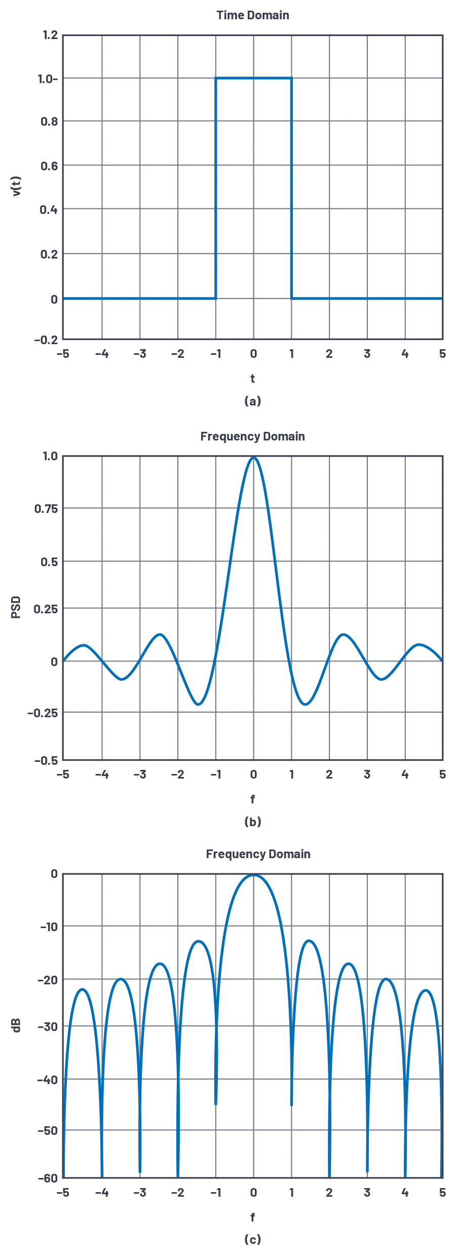
The transformation of a rectangular function in one domain to a sinc function in another domain comes up in different forms in electrical engineering. The most common form is a rectangular pulse, in time, emits the spectral content of a sinc function. It is also used in reverse, where wideband applications transform a wideband waveform to a narrow pulse in time. Phased array antennas have a similar property: a rectangular weighting along the planar axis of the array radiates a pattern following a sinc function.
For applications subjected to this property, the sidelobes of the sinc function are problematic with the first sidelobe being only –13dBc. Figure 1 illustrates this principle.
Tapering (or Weighting)
A solution to the sidelobe problem is to apply a weighting across the rectangular pulse. This is common in FFTs, and taperingoptions in phased arrays are directly analogous to weighting applied in FFTs. The unfortunate drawback of weighting is that sidelobes are reduced at the expense of widening the main lobe. Some example weighting functions are shown in Figure 2.
Waveform vs. Antenna Analogy
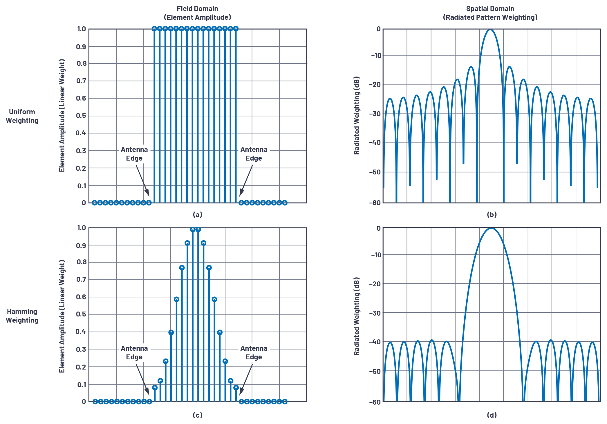
The transformation from time to frequency is routine enough that it becomes natural for most electrical engineers to visualise. However, for engineers new to phased arrays, how to use the analogy for antenna patterns may not be initially apparent. To do so, we replace the time domain signal with the field domain excitation, and the frequency domain output is replaced with the spatial domain.
Time Domain → Field Domain
Frequency Domain → Spatial Domain
Figure 3 illustrates the principle. Here we compare the radiated energy for two different weightings applied across the array. Figure 3a and Figure 3c illustrate the field domain. Each dot represents the amplitude of one element in this N = 16 array. Beyond the antenna, there is no radiated energy, and radiation begins at the antenna edge. In Figure 3a, there is an abrupt change in the field, while in Figure 3c, there is a gradual increase with distance from the antenna edge. The resulting impact on the radiated energy is shown in Figure 3b and Figure 3d, respectively.
In the next sections, we will introduce two additional error terms that impact the antenna pattern performance. The first is mutual coupling. For the purpose of this article, we merely acknowledge the problem and amount of EM modelling used to quantify the impact. The second is quantisation sidelobes due to a finite number of bits in the phase shift control. Quantisation errors are given a more in-depth treatment and quantisation sidelobes are quantified.
Mutual Coupling Errors
All the equations and array factor plots discussed here have assumed that the elements are identical and each has the same radiation pattern. In practice, this is not the case. One of the reasons for this is mutual coupling, which is the coupling between adjacent elements. An element’s radiating performance may change significantly when it is widely separated in the array vs. when it is spaced more closely. The elements at the edge of the array have a different surrounding environment than the elements in themiddle of the array. Furthermore, as the beam is steered, the mutual coupling between elements changes. All these effects createan additional error term to be accounted for by the antenna designer and, in practice, much effort is spent with electromagnetic simulators to characterise the radiation effects under these conditions.
Beam Angle Resolution and Quantisation Sidelobes
Another practical phased array antenna impairment is due to the finite resolution of the time delay unit, or phase shifter, used to steer the beam. This is typically digitally controlled with discrete time (or phase) steps. But how does one determine the resolution, or number of bits, required to achieve the beam quality goals?
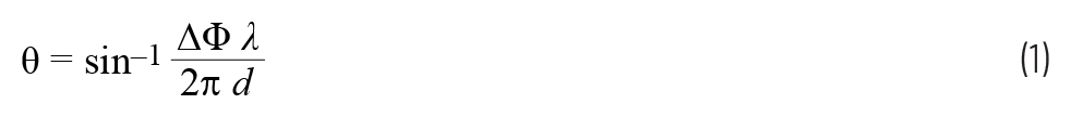
Contrary to common misconceptions, beam angle resolution is not equivalent to the resolution of the phase shifters. In Equation 1 (Equation 2 in Part 2), we saw this relationship:
We can express this in terms of the phase shift across the entire array by substituting the array width D for the element spacing d. If we then substitute the phase shifter ΦLSB for ∆Φ, we can approximate the beam angle resolution. For a linear array with N elements spaced at a half wavelength, the resolution of the beam angle is shown in Equation 2.
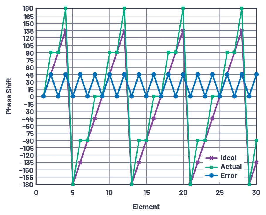
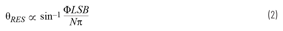 This is the beam angle resolution off boresight and describes the beam angle when one half of the array has a phase shift of zero, and the other half has a phase shift of the LSB of the phase shifter. Smaller angles are possible if less than one half of the array is programmed to the phase LSB. Figure 4 plots the beam angle for a 30-element array using a 2-bit phase shifter, as the phase LSB is progressively switched into elements from left to right across the array. Note that the beam angle increases until half of the elements are shifted by an LSB, and then returns to zero when all elements are at the LSB. This makes sense as the beam angle changes through a difference in phase across the array. Note that the peak of this characteristic is θRES, as previously calculated.
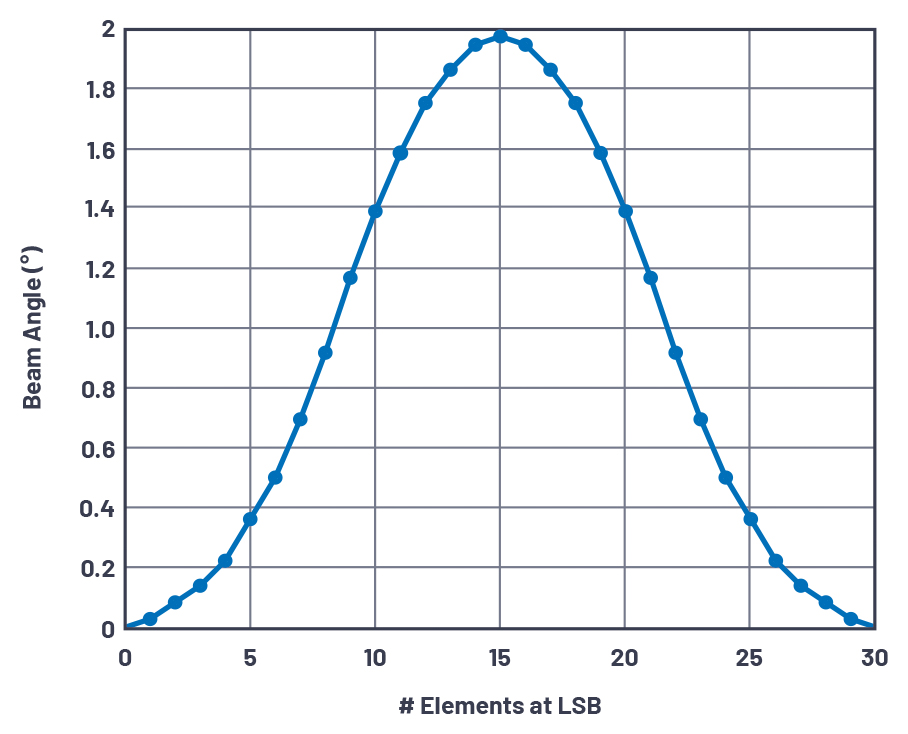
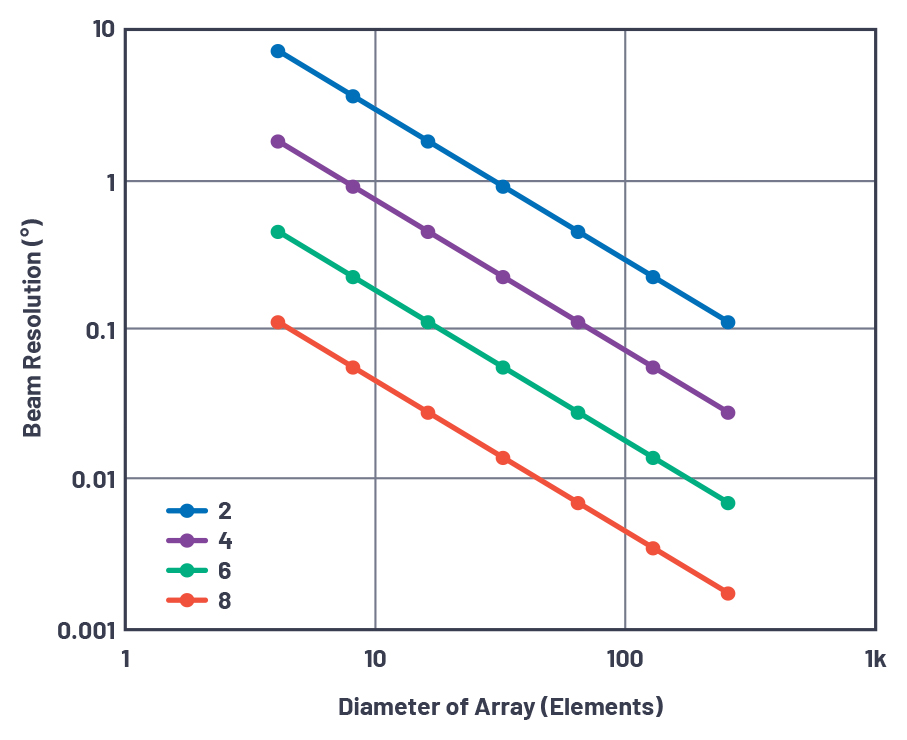
Figure 5 plots θRES as a function of array diameter (at λ/2 element spacing) for different phase shifter resolutions. This shows that even a very coarse 2-bit phase shifter with a 90° LSB can achieve 1° resolution for an array diameter of 30 elements. Solving Equation 10 in Part 1 for 30 elements at λ/2 spacing, the main lobe beamwidth is approximately 3.3°, suggesting that we haveample resolution even with this very coarse phase shifter. So, what do we get for a higher resolution phase shifter? Drawing fromanalogies between time sampled systems (data converters) and space sampled systems (phased array antennas), a higherresolution data converter produces a lower quantisation noise floor. Higher resolution phase/time shifters result in lowerquantisation sidelobe levels (QSLL).
Figure 6 shows the phase shifter settings and phase error across the 2-bit, 30-element linear array previously described, programmed to the beam resolution angle θRES. Half of the array is set to zero phase shift, and the other half is set to the 90° LSB. Note that the error, the difference between the ideal and actual quantised phase shift is sawtooth in shape.
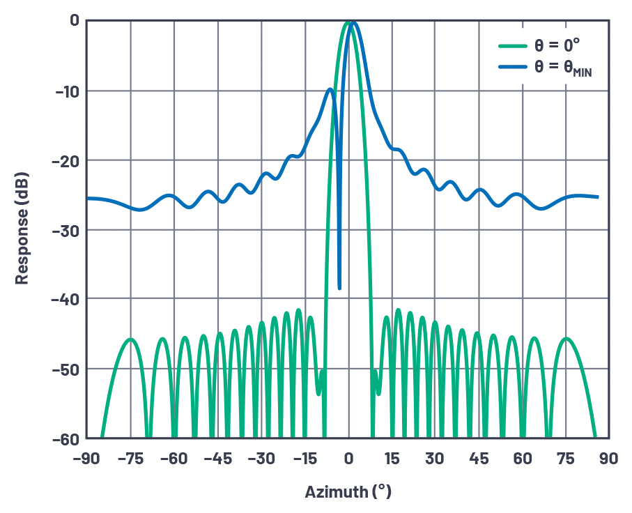
The antenna patterns for the same antenna steered to 0° and to the beam resolution angle are shown in Figure 7. Note that there is a severe degradation of the pattern due to the quantisation error of the phase shifter.
The worst-case quantisation sidelobes occur when the maximum quantisation error occurs across the aperture, when every other element is at zero error, and the neighbour is at LSB/2. This represents both the maximum possible quantisation error and the maximum periodicity of the error across the aperture. This condition is shown for the 2-bit, 30-element case in Figure 8.
This situation occurs at predictable beam angles as shown in Equation 3.
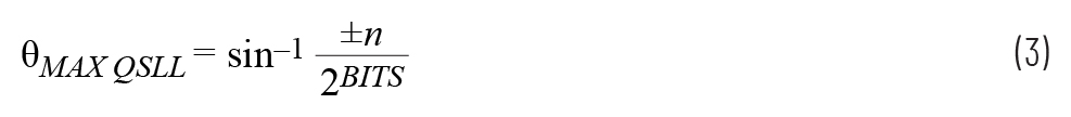
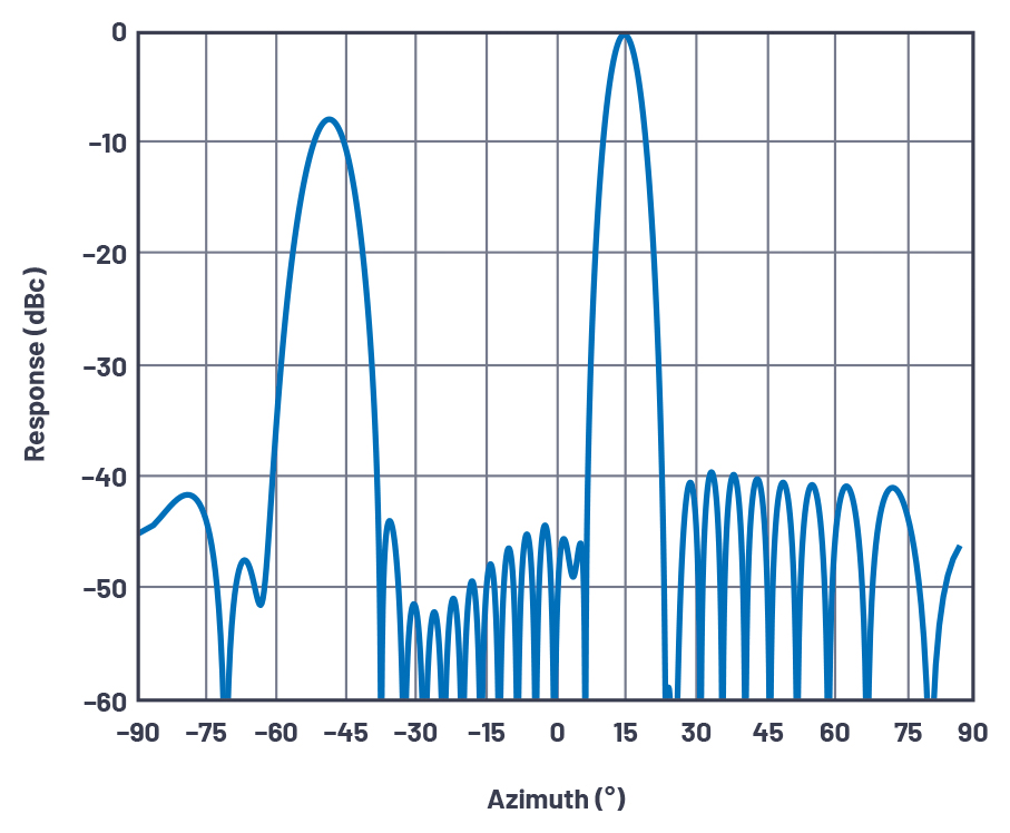
where n < 2BITS, and n is odd. For a 2-bit system, this condition is satisfied four times between horizons, at ±14.5° and ±48.6°. Figure 9 shows the antenna pattern for this system for n = 1, q = +14.5°. Note the substantial –7.5dB quantisation sidelobe at –50°.
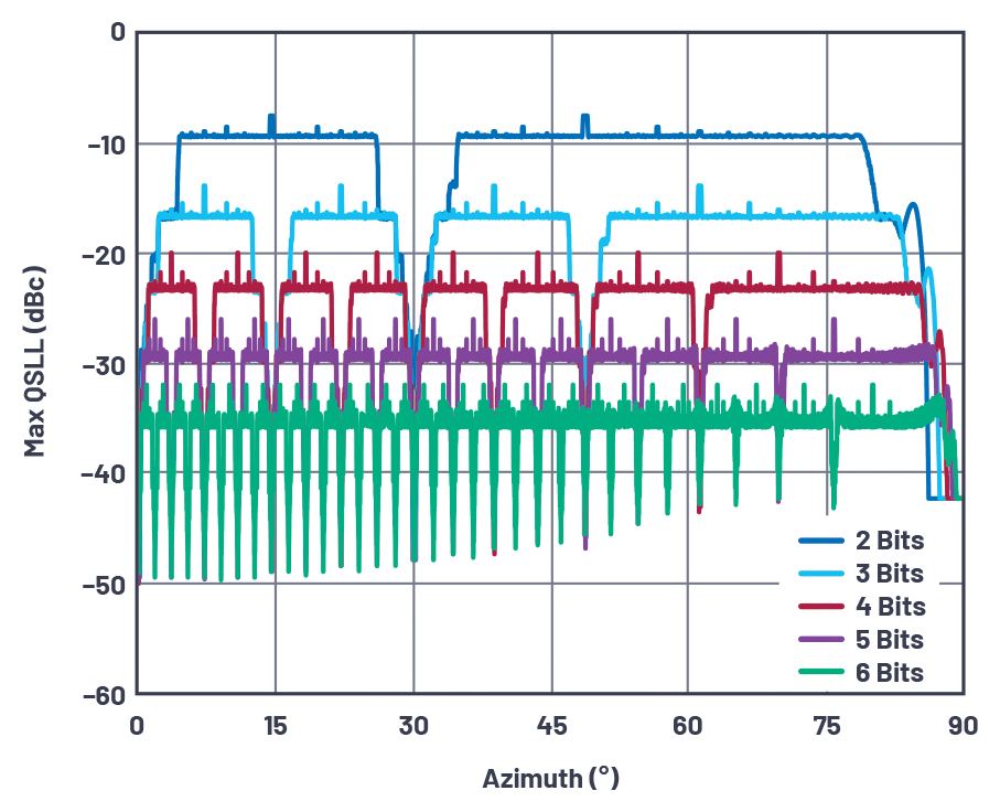
At beam angles other than the special cases where the quantisation error is sequentially 0 and LSB/2, the rms error is reduced as it is spread across the aperture. In fact, for the angle equation (Equation 3) for even values of n, the quantisation error is zero. If we plot the relative level of the highest quantisation sidelobe for various phase shifter resolutions, some interesting patterns emerge. Figure 9 shows the worst-case QSLL for a 100-element linear array, employing a Hamming taper so that the quantisation sidelobescan be differentiated from the classical windowing sidelobes discussed earlier in this section.
Note that at 30°, all quantisation error goes to zero, which can be shown to be a consequence of sin(30°) = 0.5. Notice that the beam angle of the worst-case level for any particular n-bit phase shifter exhibits zero quantisation error at any higher resolution n. The beam angles for worst-case sidelobe levels described here can be seen, as well as the 6dB improvement in QSLL per bit ofresolution.
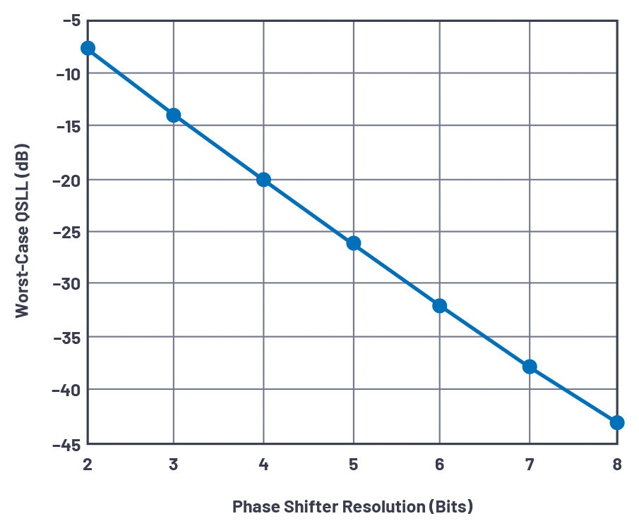
The maximum quantisation sidelobe levels, QSLL, for 2-bit to 8-bit phase shifter resolutions are shown in Figure 11, which follows the familiar quantisation noise law for data converters,

or about 6dB per bit of resolution. At 2 bits, the QSLL levels are about –7.5dB, higher than the classical +12dB for a data converter sampling a random signal. This discrepancy can be viewed as a consequence of the periodically occurring sawtooth error being sampled across the aperture, where the spatial harmonics add in phase. Note that the QSLL is not a function of the aperture size.
Closing Comments
We can now summarise some of the challenge’s antenna engineers face relative to beamwidth and sidelobes:
This concludes a three-part series on phased array antenna patterns. In Part 1, we introduced beam pointing, array factor, andantenna gain. In Part 2, we introduced imperfections of grating lobes and beam squint. In Part 3, we discussed tapering and quantisation errors. The intention is aimed not for antenna design engineers fluent in electromagnetic and radiating elementdesign, but rather the large number of engineers in adjacent disciplines working on phased arrays who may benefit from an intuitive explanation of the varied impacts affecting the overall antenna pattern performance.
Analog Devices: www.analog.com
References
Balanis, Constantine A. Antenna Theory, Analysis and Design. Third edition. Wiley, 2005.
Mailloux, Robert J. Phased Array Antenna Handbook. Second edition. Artech House, 2005.
O’Donnell, Robert M. “Radar Systems Engineering: Introduction.” IEEE, June 2012. Skolnik, Merrill. Radar Handbook. Third edition. McGraw Hill, 2008.
About the Author
Peter Delos is a technical lead in the Aerospace and Defense Group at Analog Devices in Greensboro, NC. He received his B.S.E.E. from Virginia Tech in 1990 and M.S.E.E. from NJIT in 2004. Peter has over 25 years of industry experience. Most of his career has been spent designing advanced RF/analogue systems at the architecture level, PWB level, and IC level. He is currently focused on miniaturising high performance receiver, waveform generator, and synthesiser designs for phased array applications. He can be reached at peter.delos@analog.com.
About the Author
Bob Broughton started at Analog Devices in 1993 and has held positions as a product engineer and an IC design engineer, and is currently the director of engineering in the Aerospace and Defense Business Unit. Prior to ADI, Bob worked at Raytheon as an RF design engineer and at Peregrine Semiconductor as an RFIC designer. Bob graduated with a B.S.E.E. from West Virginia University in 1984. He can be reached at bob.broughton@analog.com.
About the Author
Jon Kraft is a senior staff FAE in Colorado and has been with ADI for 13 years. His focus is software-defined radio and aerospace phased array radar. He received his B.S.E.E. from Rose-Hulman and his M.S.E.E. from Arizona State University. He has ninepatents issued, six with ADI, and one currently pending. He can be reached at jon.kraft@analog.com.


McMurtry Spéirling defies gravity using fan downforce
Ground effect fans were banned from competitive motorsport from the end of the 1978 season following the introduction of Gordon Murray's Brabham...