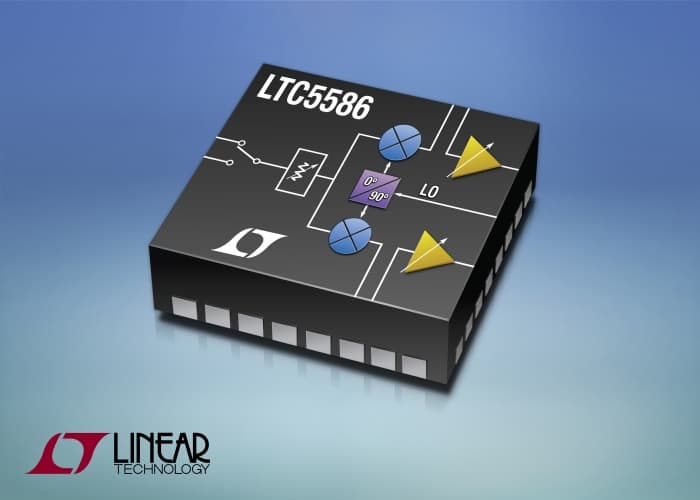
Linear Technology has introduced a new high linearity I/Q demodulator, the LTC5586, with more than 1GHz, –1dB flatness bandwidth, supporting next-generation 5G wireless infrastructure equipment such as DPD (digital predistortion correction) receivers for base stations, microwave backhaul and software-defined radios (SDR), as well as other broadband receiver applications. The LTC5586’s RF input port is truly broadband. With a single network, it is 50Ω matched from 500MHz to 6GHz, covering all the LTE bands, as well as the emerging 4.5G and 5G bands at 3.6GHz and 5GHz. For operation from 300MHz to 500MHz, an additional capacitor does the job. The device also has built-in SPI tunability, allowing the demodulator to set its LO input to any frequency band from 300MHz to 6GHz with no external matching components. The new demodulator supports very high OIP2 of 80dBm and 60dBc sideband suppression, ensuring superior receiver performance.
The LTC5586 is a true zero-IF design that demodulates wideband RF signals directly to baseband DC or low IF coupling. The demodulator exploits the quadrature relationship between the two I and Q channels, sufficiently containing all the information available when both channels are sampled at one-half the bandwidth of the full RF bandwidth from which they came. As a result, the A/D converters’ (ADC) sampling rate and cost can be reduced.
In the front end, the LTC5586 has an RF switch that selects one of its two inputs to a programmable attenuator via the on-chip serial bus. This front-end attenuator has a gain-control range of 31dB in 1dB steps, allowing the receiver to accommodate a wide range of signal inputs. The demodulator consists of I and Q mixers, with their respective LO driven by an accurate wideband quadrature phase shifter. After the signal is demodulated, two programmable gain amplifiers provide gains to the I and Q baseband signal paths. Maximum gain of 7.7dB can be set by the serial port in 1dB steps, allowing users to optimally set the signal levels while driving a pair of external A/D converters directly.
Additionally, the LTC5586 has a unique on-chip tuning facility for simple calibration via the SPI serial port. Through this interface, the user can adjust the I and Q amplitude and phase balance, resulting in a much simplified calibration to attain unprecedented 60dBc or better image rejection performance. The same interface can optimise the IIP2, IIP3, HD2 (2nd harmonic distortion) and HD3 performance, improving the overall linearity performance of a receiver. With the device’s baseband DC coupled, its DC offset voltage can be zeroed, including the entire baseband signal chain, so long as the combined total offset is within the adjustment range of the LTC5586.
The LTC5586 comes in a 5 x 5mm plastic QFN package. The I and Q outputs are able to drive directly into a pair of interstage filters and external ADCs when terminated externally with a 100Ω differential impedance. This results in a compact solution, requiring few external components. Operating temperature range is specified from –40°C to 105°C case. The LTC5586 is priced starting at $7.79 each in 1,000-piece quantities and is now available in production quantities.


McMurtry Spéirling defies gravity using fan downforce
Ground effect fans were banned from competitive motorsport from the end of the 1978 season following the introduction of Gordon Murray's Brabham...