Introduction
Designing the correct power source is essential and complex, since there is no one typical application. While total automation of power supply design is yet to be achieved, a comprehensive range of semi-automated tools are available today. This article details the use of semi-automated design tools through five critical steps of the power supply design process. These tools can be valuable to both the novice and expert power supply design engineer.
Power Supply Design Step 1: Creating the Power Supply Architecture
Creating a suitable power supply architecture is a decisive step in power supply design. This step becomes more complex by increasing the number of needed voltage rails. At this point, the decision is made as to whether and how many intermediate circuit voltages need to be created. Figure 1 shows a typical block diagram of a power supply. The 24V supply voltage of an industrial application is shown on the left. This voltage must be converted now into 5V, 3.3V, 1.8V, 1.2V, and 0.9V with corresponding currents. What is the best method for generating the individual voltages? Selecting a classic step-down switching (buck) converter makes the most sense for converting from 24V to 5V. However, how do you generate the other voltages? Does it make sense to generate the 3.3V from the 5V already created, or should we convert to 3.3V directly from 24V? Answering these questions requires further analysis. Since an important property of a power supply is the conversion efficiency, keeping the efficiency as high as possible is important when selecting the architecture.
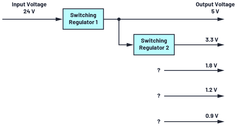
If intermediate voltages, such as 5V in the example shown in Figure 1, are used to generate additional voltages, the energy used for the 3.3V must already pass through two conversion stages. Each conversion stage has only limited efficiency. If, for example, a conversion efficiency of 90% is assumed for each conversion stage, the energy for 3.3V, which has already passed through two conversion stages, only has an efficiency of 81% (0.9 × 0.9 = 0.81). Can this rather low efficiency be tolerated in a system or not? This depends on the current required from this 3.3V rail. If current of only a few mA is needed, the low efficiency might not be a problem at all. For higher currents, however, this lower efficiency might have a greater effect on the overall system efficiency and consequently represent a big disadvantage.
From the considerations just mentioned, however, you cannot draw the general conclusion that it is always better to convert directly from a higher supply voltage to the lower output voltage in one step. Voltage converters that can handle a higher input voltage are usually more expensive and have a reduced efficiency when there is a greater difference between the input voltage and the output voltage.
In power supply design, the solution to finding the best architecture is to use an architecture tool such as LTpowerPlanner®. It is available free of charge from Analog Devices and is part of the LTpowerCAD® development environment, which can be installed locally on your computer. LTpowerPlanner is a tool that makes evaluating different architectures quick and easy.
Finalising the Specification
Finalising the specification is extremely important in power supply design. All additional development steps depend on the specification. Frequently, the precise requirements of the power supply are unknown until the rest of the electronic system has been completely designed. This usually results in increasing time constraints on power supply design development. It also often happens that the specification is changed in a later development stage. For example, if in its final programming, an FPGA requires additional power, the voltage for a DSP must be reduced to save energy, or the originally intended switching frequency of 1MHz must be avoided because it is coupled into the signal path. Such changes can have very serious effects on the architecture and, in particular, on the circuit design of the power supply.
A specification is usually adopted at an early stage. This specification should be designed to be as flexible as possible so that it is relatively easy to implement any changes. In this effort, selecting versatile integrated circuits is helpful. Working with development tools is particularly valuable. This allows the power supply to be re-calculated within a short time. In this way, specification changes can be implemented more easily and, above all, more quickly.
The specification includes the available energy, the input voltage, the maximum input current, and the voltages and currents to be generated. Other considerations include size, financial budget, thermal dissipation, EMC requirements (including both conducted and radiated behaviours), expected load transients, changes in the supply voltage, and safety.
LTpowerPlanner as an Optimisation Aid
LTpowerPlanner provides all the necessary functions for creating a power supply system architecture. It is very simple to operate, allowing for rapid concept development.
An input energy source is defined and then individual loads, or electrical consumers, are added. This is followed by adding individual dc-to-dc converter blocks. These could be switching regulators or low dropout (LDO) linear regulators. All components can be assigned their own name. An expected conversion efficiency is stored for efficiency calculations.
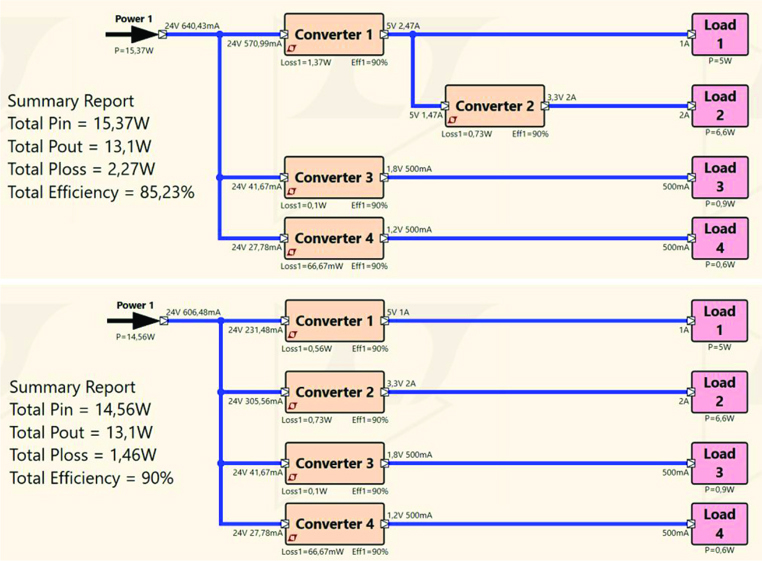
Using LTpowerPlanner has two great benefits. First, a simple architecture calculation can identify the configuration of the individual conversion stages most beneficial for overall efficiency. Figure 2 shows two different architectures for the same voltage rails. The architecture at the bottom has an overall efficiency that is somewhat higher than that of the architecture at the top. This property is not evident without a detailed calculation. When using LTpowerPlanner, this difference is immediately revealed.
The second benefit of LTpowerPlanner is that it provides well-organised documentation. The graphical user interface provides a neat sketch of the architecture, a visual aid that can be invaluable in discussions with co-workers and in documenting the development effort. Documentation can be stored either as a paper hard copy or a digital file.
Power Supply Design Step 2: Selecting Integrated Circuits for Each DC-to-DC Converter
When designing power supplies today, an integrated circuit is used rather than a discrete circuit with many separate components. There are a multitude of different switching regulator ICs and linear regulators available in the market. All of them are optimised for one specific property. Interestingly, all integrated circuits are different and can be interchanged only in the rarest of cases. Selecting the integrated circuit thus becomes a very important step. Once an integrated circuit has been selected, the properties of that circuit are fixed for the rest of the design process. Later, if it turns out that a different IC is better suited, the effort to incorporate a new IC begins again. This development effort can be very time consuming but can be easily mitigated with the use of design tools.
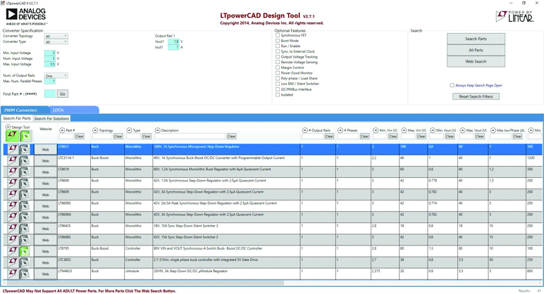
Using a tool is critical for effectively selecting the integrated circuit. The parametric search on analog.com is suitable for this. Searching for components within LTpowerCAD can be even more productive. Figure 3 shows the search window.
To use the search tool, only a few specifications need to be entered. For example, you may enter the input voltage, output voltage, and required load current. Based on these specifications, LTpowerCAD generates a list of recommended solutions. Additional criteria can be entered to further narrow down the search. For example, in the Features category you can select from features such as an enable pin or galvanic isolation to find an appropriate dc-to-dc converter.
Power Supply Design Step 3: Circuit Design of the Individual DC-to-DC Converters
Step 3 is the circuit design. The external, passive components need to be selected for the chosen switching regulator IC. The circuit is optimised in this step. Usually, this requires studying a data sheet thoroughly and performing all the required calculations. This step in power supply design can be drastically simplified by the comprehensive design tool, LTpowerCAD, and the results can be optimised further.
LTpowerCAD as a Powerful Calculation Tool
LTpowerCAD was developed by Analog Devices to greatly simplify circuit design. It is not a simulation tool, but rather a calculation tool. It recommends, in a very short time, the optimised external components based on the specification entered. The conversion efficiency can be optimised. The transfer function of the control loop is also calculated. This makes it easy to implement the best control bandwidth and stability.
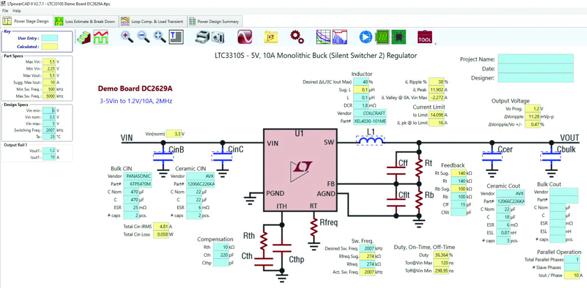
After opening a switching regulator IC in LTpowerCAD, the main screen displays the typical circuit with all the necessary external components. Figure 4 shows this screen for the LTC3310S as an example. This is a step-down switching regulator with an output current of up to 10A and a switching frequency of up to 5MHz.
The yellow fields on the screen show the calculated or specified values. The user can configure settings using the blue fields.
Selecting the External Components
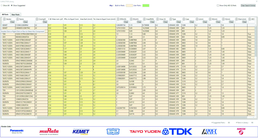
LTpowerCAD reliably simulates the behaviours of a real circuit as calculations are based on detailed models of external components, not just ideal values. LTpowerCAD includes a large database of integrated circuit models from several manufacturers. For instance, the equivalent series resistance (ESR) of a capacitor and the core losses of a coil are taken into consideration. To select external components, click on a blue external component as shown in Figure 4. A new window will open, showing a long list of possible components. As an example, Figure 5 shows a list of recommended output capacitors. This example shows a selection of 88 different capacitors from various manufacturers. You can also exit the list of recommended components and select the Show All option to choose from a variety of more than 4660 capacitors.
This list is continuously expanded and updated. While LTpowerCAD is an offline tool and does not require internet access, regular software updates (using the update function) will ensure that the integrated switching regulator ICs and the database of external components remain up to date.
Checking the Conversion Efficiency
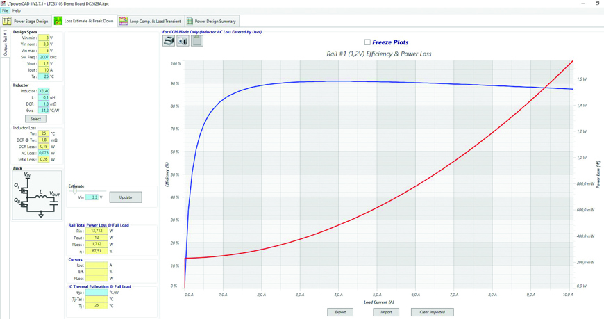
Once the optimal external components have been selected, the conversion efficiency of the switching regulator is checked using the Loss Estimate & Break Down button.
A precise diagram of the efficiency and losses is then displayed. In addition, the junction temperature reached in the IC can be calculated based on the thermal resistance of the housing. Figure 6 shows the page of calculations for the conversion efficiency and thermal behaviour.
Once you are satisfied with the circuit response, you can move to the next set of calculations. If the efficiency is not satisfactory, the switching frequency of the switching regulator can be changed (see left side of Figure 6), or the selection of the external coil can be changed. The efficiency is then recalculated until a satisfactory result is achieved.
Optimising the Control Bandwidth and Checking the Stability
After selecting the external components and calculating the efficiency, the control loop is optimised. The loop must be set so that the circuit is reliably stable, not prone to oscillations or even instability while providing a high bandwidth - that is, the ability to respond to changes of the input voltage and, in particular, to load transients. The stability considerations in LTpowerCAD can be found in the Loop Comp. & Load Transient tab. In addition to a Bode plot and curves on the response of the output voltage following load transients, there are many setting options.
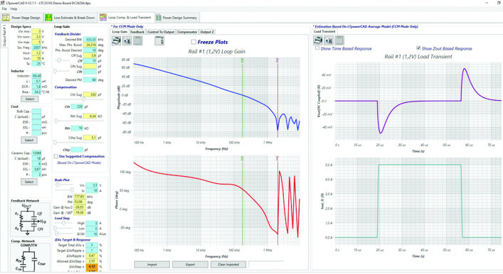
The Use Suggested Compensation button is the most important. In this case, the optimised compensation is used, and the user need not dive deeply into control engineering to adjust any parameters. Figure 7 shows the LTpowerCAD screen when setting the control loop.
The stability calculations performed in LTpowerCAD are a highlight of its architecture. The calculations are performed in the frequency domain and are very fast, much faster than simulations in the time domain. As a result, parameters can be changed on a trial basis and an updated Bode plot is provided in a few seconds. For a simulation in the time domain, this would take many minutes or even hours.
Checking the EMC Response and Adding Filters
Depending on the specification, additional filters may be necessary at the input or output of the switching regulator. This is where less experienced power supply developers, in particular, face large challenges. The following questions arise: How must the filter components be selected to ensure a certain voltage ripple at the output? Is an input filter necessary and, if so, how must this filter be designed to keep conducted emissions below certain EMC limits? In this respect, interaction between the filter and the switching regulator must not result in instability under any circumstances.
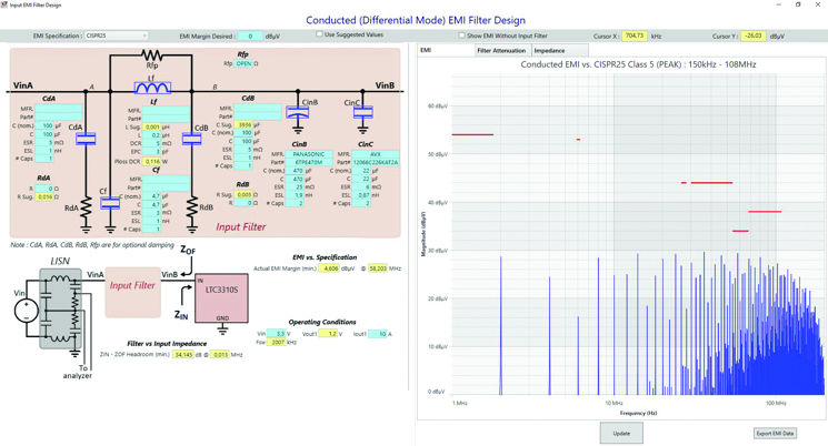
Figure 8 shows the Input EMI Filter Design, which is a sub-tool in LTpowerCAD. This can be accessed from the first page where the external, passive components are optimised. Starting the filter designer brings up a filter design using passive ICs and an EMC graph. This graph plots the conducted interference with or without an input filter and within appropriate limits from various EMC specifications such as CISPR 25, CISPR 22, or MIL-STD-461G.
The filter characteristic in the frequency domain and the filter impedance can also be displayed graphically beside the illustration of the input conducted EMC response. This is important to ensure that a filter does not have total harmonic distortion that is too high, and that the filter impedance matches the impedance of the switching regulator. Problems with the impedance match can lead to instabilities between the filter and the voltage converter.
Such detailed considerations can be accounted for in LTpowerCAD and do not require in-depth knowledge. With the Use Suggested Values button, the filter design is automated.
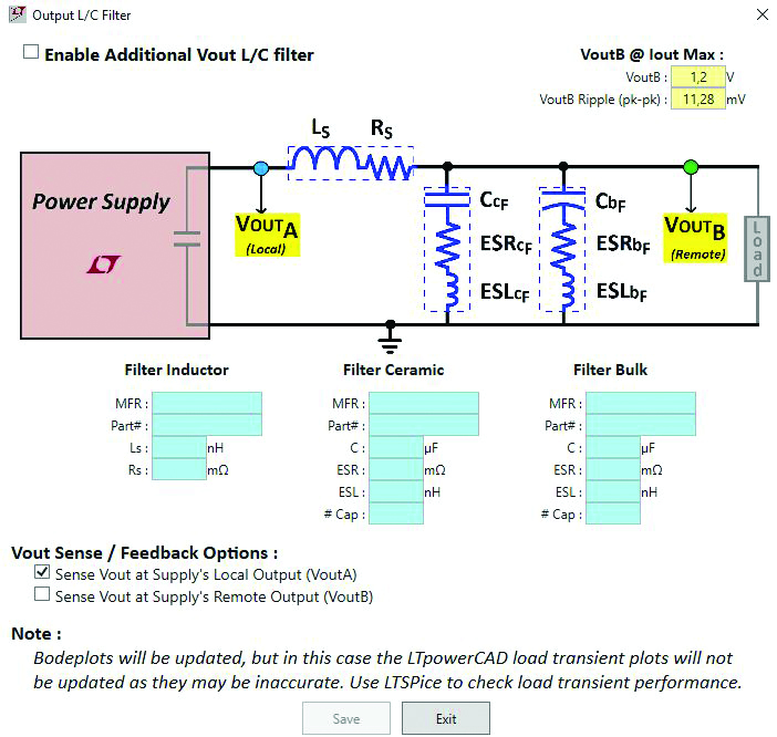
Of course, LTpowerCAD also supports the use of a filter on the output of the switching regulator. This filter is often used for applications where the output voltage is only allowed to have a very low output voltage ripple. To add a filter in the output voltage path, click the LC filter icon on the Loop Comp. & Load Transient page. Once this icon is clicked, a filter appears in a new window, as shown in Figure 9. The parameters of the filter can be easily selected here. The feedback loop can either be connected in front of this additional filter or behind it. Here, a stable response of the circuit can be ensured in all operating modes despite very good dc precision of the output voltage.
Power Supply Design Step 4: Simulation of the Circuit in the Time Domain
Once you have completely designed a circuit using LTpowerCAD, simulating it is the crowning achievement. Simulations are usually run in the time domain. Individual signals are checked against time. The interaction of different circuits can also be tested on a printed circuit board. It is also possible to integrate parasitic effects into the simulation. With this, the result of the simulation becomes very accurate, but the simulation times are longer.
Generally, a simulation is suitable for collecting additional information prior to implementing real hardware. It is important to know the potential and the limits of circuit simulation. Finding the optimal circuit might not be possible using simulation only. During simulation, one can modify parameters and restart the simulation. However, if the user is not an expert in designing circuits, it can be difficult to determine the right parameters and then to optimise them. As a result, it is not always clear to the user of a simulation whether the circuit has already achieved the optimal state. A computing tool such as LTpowerCAD is better suited for this purpose.
Simulating the Power Supply Using LTspice
LTspice®, from Analog Devices, is a powerful simulation programme for electric circuits. It is very widely used by hardware developers globally, due to its ease of use, extended network of user support, optimisation options, and high quality, reliable simulation results. Additionally, LTspice is free of charge and can easily be installed on a personal computer.
LTspice is based on the SPICE programme, which originated from the Department of Electrical Engineering and Computer Sciences at the University of California, Berkeley. The acronym SPICE stands for simulation programme with integrated circuit emphasis. Many commercial versions of this programme are available. Although originally based on Berkeley’s SPICE, LTspice offers considerable improvements in the convergence of circuits and simulation speed. Additional features of LTspice include a circuit diagram editor and waveform viewer. Both are intuitive to operate, even for a beginner. These features also provide a great deal of flexibility for the experienced user.
LTspice is designed to be simple and easy to use. The programme, available for download at analog.com, includes a very large database containing simulation models of nearly all power ICs from Analog Devices along with external passive components. As mentioned, once installed, LTspice can operate offline. However, regular updates will ensure that the newest models of switching regulators and external components are loaded.
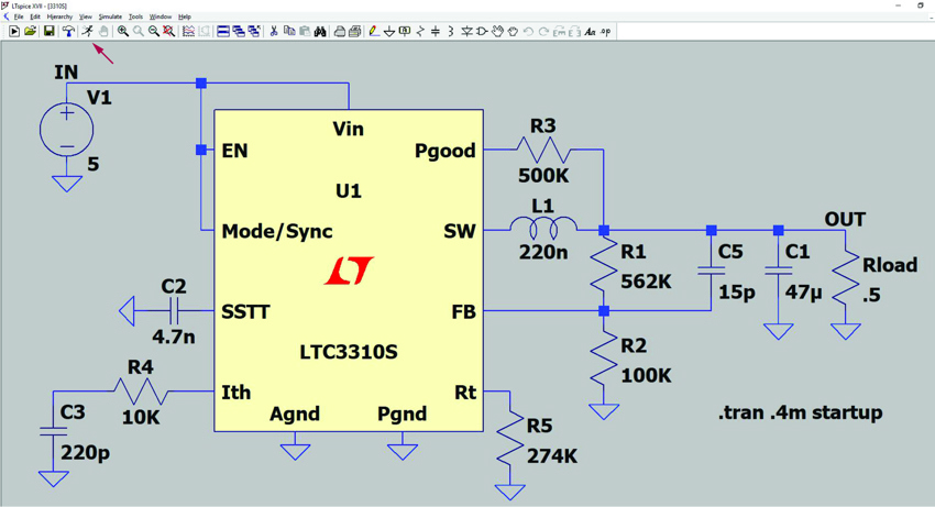
To start an initial simulation, choose an LTspice circuit in the product folder of a power product on analog.com (for example, the LT8650S evaluation board). These are usually the suitable circuits of the available evaluation boards. By double-clicking the related LTspice link in a specific product folder on analog.com, LTspice will launch the complete circuit locally on your PC. It includes all external components and presets necessary to run a simulation. Then, click on the runner icon, pictured in Figure 10, to start simulation.
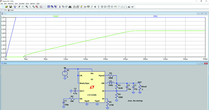
Following a simulation, all the voltages and currents of a circuit can be accessed using the waveform viewer. Figure 11 shows a typical illustration of the output voltage and the input voltage as the circuit ramps up.
A SPICE simulation is primarily suited for getting to know a power supply circuit in detail so that there are no unwanted surprises when building the hardware. A circuit can also be changed and optimised using LTspice. In addition, the interaction of the switching regulator with the other parts of the circuit on the printed circuit board can be simulated. This is particularly helpful in uncovering interdependencies. For example, several switching regulators can be simulated at the same time in one run. This extends the simulation time, but certain interactions can be checked in this case.
Finally, LTspice is an extremely powerful and reliable tool used by IC developers today. Many ICs from Analog Devices have been developed with the help of this tool.
Power Supply Design Step 5: Testing the Hardware
While automation tools have a valuable purpose in power supply design, the next step is to perform a basic hardware evaluation. The switching regulator operates with currents switched at a very high rate. Due to the parasitic effects of the circuit - particularly of the printed circuit board layout - these switched currents cause voltage offset, which generates radiation. Such effects can be simulated using LTspice. To do this, however, you need precise information about the parasitic properties. Most of the time this information is not available. You would have to make many assumptions, and these reduce the value of the simulation result. Consequently, a thorough hardware evaluation must be completed.
Printed Circuit Board Layout - An Important Component
The printed circuit board layout is usually known as a component. It is so critical that, for example, it is not possible to operate a switching regulator for test purposes using jumper wires, as it is with a breadboard. Mainly, the parasitic inductance in the paths where the currents are switched leads to a voltage offset that makes operation impossible. Some circuits could also be destroyed due to excessive voltage.
There is support available for creating an optimal printed circuit board layout. The corresponding data sheets for the switching regulator ICs usually provide information about a reference printed circuit board layout. For most applications, this suggested layout can be used.
Evaluating the Hardware Within the Specified Temperature Range
During the power supply design process, conversion efficiency is considered to determine whether the switching regulator IC operates within the permissible temperature range. However, testing the hardware at its intended temperature limits is important. The switching regulator IC and even the external components vary their rated values over the permissible temperature range. These temperature effects can easily be taken into consideration during the simulation using LTspice. However, such a simulation is only as good as the given parameters. If these parameters are available with realistic values, LTspice can perform a Monte Carlo analysis that leads to the desired result. In many cases, evaluating the hardware through physical testing is still more practical.
EMI and EMC Considerations
In late stages of system design, hardware must pass electromagnetic interference and compatibility (EMI and EMC) tests. While these tests must be passed with real hardware, simulation and calculation tools can be extremely useful in gathering insights. Different scenarios can be evaluated prior to hardware testing. Certainly, there are some parasitics involved that are usually not modelled in simulation, but general performance trends related to these test parameters can be obtained. Additionally, the data obtained from such simulations can provide the insights necessary to apply modifications to the hardware quickly, in case an initial EMC test was not passed. Since EMC tests are costly and time intensive, utilising software such as LTspice or LTpowerCAD in early design stages can help achieve more accurate results prior to testing, thus speeding up the overall power supply design process and reducing costs.
Summary
The tools available for power supply design have become very sophisticated and powerful enough to meet the demands of complex systems. LTpowerCAD and LTspice are high performance tools with simple to use interfaces. As a result, these tools can be invaluable to a designer with any level of expertise. Anyone from the experienced developer to the less experienced can use these programmes to develop power supplies on a day-to-day basis.
It is astounding how much simulation capabilities have evolved. Using the proper tools can help you build a reliable, sophisticated power supply more quickly than ever before.
The Free Power Tools from ADI
Follow these links:
Analog Devices: www.analog.com
About the Author
Frederik Dostal is a power management expert with more than 20 years of experience in this industry. After his studies of microelectronics at the University of Erlangen, Germany, he joined National Semiconductor in 2001, where he worked as a Field Applications Engineer, gaining a lot of experience in implementing power management solutions in customer projects. During his time at National, he also spent four years in Phoenix, Arizona (USA), working on switch mode power supplies as Applications Engineer. In 2009, he joined Analog Devices, where since then he held a variety of positions working for the product line, European technical support and currently brings in his broad design and application knowledge as Power Management Expert. Frederik is working out of the Analog Devices office in Munich, Germany. He can be reached at frederik.dostal@analog.com.


McMurtry Spéirling defies gravity using fan downforce
Ground effect fans were banned from competitive motorsport from the end of the 1978 season following the introduction of Gordon Murray's Brabham...