
Time-of-flight (ToF) cameras have gained attention as the depth sensing method of choice for its smaller form factor, wide dynamic range of sensing, and its ability to operate in a variety of environments. Though ToF technology has been used for years in the scientific and military fields, it has become more prevalent starting in the early 2000s with advances in image sensing technology. This evolution in performance means that technologies such as ADI’s ToF technology will become more ubiquitously deployedbeyond the consumer market, where it is currently being designed into smart phones, consumer devices, and gaming devices. As the technology matures, there will be opportunities to further leverage mainstream manufacturing processes to increase system efficiencies in the design, manufacturing, and transport of goods.
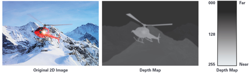
Logistics, quality inspection, navigation, robotics, facial recognition, security, surveillance, safety, healthcare, and driver monitoringare all application use cases that can leverage 3D depth sensing ToF technology to solve many problems that traditional 2Dtechnology struggles with today. Combining high resolution depth data with powerful classification algorithms and AI will uncover new applications.
This article will examine the basics of, and the two dominant methods for, ToF depth sensing, as well as compare it to other prevalent depth sensing technologies. It will then provide a detailed introduction to ADI’s 3D depth sensing ToF technology - leveraging the ADDI9036 analogue front end, a complete ToF signal processing device that integrates a depth processor that processes the raw image data from a VGA CCD sensor into depth/ pixel data. We will also discuss how ADI can scale this technology to our broad market customer base through an ecosystem of hardware partners.
Basic Theory of Operation
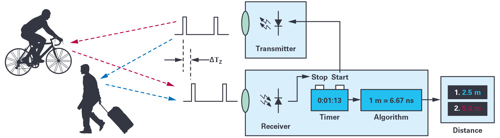
A ToF camera measures distance by actively illuminating an object with a modulated light source (such as a laser or an LED), anda sensor that is sensitive to the laser’s wavelength captures the reflected light (Figure 2). The sensor measures the time delay ∆Tbetween when the light is emitted and when the reflected light is received by the camera. The time delay is proportional
to twice the distance between the camera and the object (round-trip); therefore the depth can be estimated as:

where c is the speed of light. The goal of a ToF camera is to estimate the delay between the emitted signal and the return signal.
There are different methods for measuring ∆T, of which two have become the most prevalent: the continuous-wave (CW) method and the pulse-based method.
Continuous-Wave Method
In the CW method, a periodic modulated signal is used for the active illumination (Figure 3), and the phase shift of the reflected light is measured by homodyne demodulation of the received signal.
For example, a sinusoidal modulation can be used, where the emitted signal is:

where
The received signal r(t) is a delayed and attenuated version of the emitted signal:

where Tmod is the modulation period.
0 ≤ α <1 is an attenuation coefficient that depends on the distance and the surface reflectivity, and ∆T is the delay of the return signal.
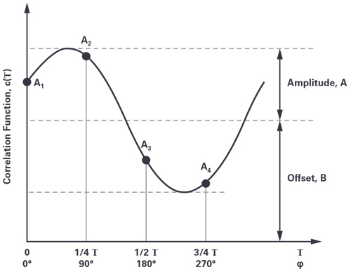
Continuous-wave time-of-flight sensors measure the distance at each pixel by sampling the correlation function between the received signal r(t) and a demodulating signal g(t) with the same frequency as s(t). In the ideal case, the demodulating signal is also a sine wave:

The operation performed by the pixel is a correlation operation:

When both the emitted signal and the demodulating signal are sine waves, the correlation value as a function of the delay τ applied to the demodulating signal is:

where A = AgAsα and B = αBgBs.
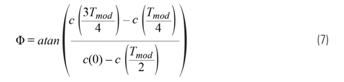
The correlation function c(τ) is then sampled at four equal steps over one period (by changing the illumination phase shift in stepsof 90°), as shown in Equation 3. The phase offset Φ = 2πfmod∆T between the emitted signal and the demodulating signal can be estimated using Equation 7:
and the depth, which is proportional to the phase shift is:

Pulse-Based Method
In the pulse-based method, an illumination source emits a series of N short light pulses, which are reflected back to a sensor equipped with an electronic shutter that enables the capture of light in a series of short temporal windows. In Figure 5, three shutter windows, or pulses, are used to capture the reflected light pulse. The BG window captures the ambient light, which is then subtracted from the other measurements.
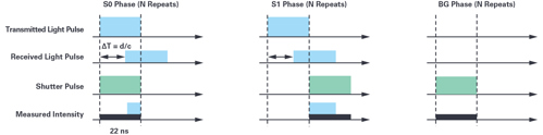
The ToF ∆T is estimated from the measured values corresponding to the different shutter windows according to the following equation:

The distance can then be calculated by replacing ∆T with the expression in Equation 9 in Equation 1, which gives us Equation 10:

It should be noted that these equations are predicated on the assumption that the pulses are perfect rectangular pulses, which is impossible, considering the limitations of the hardware. Additionally, in practical situations, several hundred to several thousand illumination pulses need to be accumulated in order to get a sufficient signal-to-noise ratio (SNR) for measurement.
Advantages/Disadvantages of the CW and Pulsed ToF Technology Systems
Both approaches to ToF have their advantages and disadvantages relative to the application’s use case. Issues such as the distances being measured, the environment in which the system is being used, accuracy requirements, thermal/power dissipationrestrictions, form factor, and power supply issues need to be considered. It should be noted that the vast majority of CW ToF systems that have been implemented and are currently on the market use CMOS sensors, while pulsed ToF systems use non-CMOS sensors (notably CCDs). For this reason, the advantages/disadvantages listed as follows will be based on those assumptions:
Advantages of Continuous-Wave Systems:
Disadvantages of Continuous-Wave Systems:
Advantages of Pulse-Based ToF Technology Systems:
Disadvantages of Pulse-Based ToF Technology Systems:
Other Depth Sensing Technologies
It is instructive to be familiar with other depth mapping technologies to understand the trade-offs; as previously mentioned, all depth detection systems have advantages and disadvantages depending on the use case and the application requirement.
Stereo Vision
Stereo vision for depth sensing works by using more than one camera separated by a certain amount of distance from one another (Figure 6). Like the human eye, a given reference point in space will be in separate positions in each camera, allowing the system to calculate that point’s position in space if the correspondence of that point is made between the two cameras. Determination of this correspondence involves computationally intense and complex algorithms.
Advantages
Disadvantages
Structured Light
The structured light method works by projecting a known reference pattern of dots onto an object. The 3D object distorts this reference pattern, and a 2D camera captures this distortion. This distortion is then compared to the reference pattern that wasprojected, and then calculates a depth map based on the distortion level.
Advantages
Disadvantages
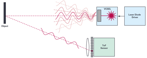
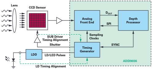
ADI Depth Sensing (ToF) Technology
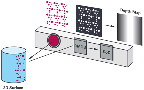
ADI’s ToF technology is a pulse-based ToF CCD system (Figure 8) that utilises a high performance ToF CCD and the ADDI9036, a complete ToF signal processing device that integrates a 12-bit ADC, the depth processor (that processes the raw image data from the CCD into depth/pixel data), as well as a high precision clock generator that generates the timing for both the CCD and the laser. The precision timing core of the timing generator allows the adjustment of clocks and LD output with approximately 174ps resolution at a clock frequency of 45MHz.
ADI’s ToF system differentiates itself from other solutions by:
A pseudo-randomisation algorithm combined with special image processing integrated in the depth processor enables interference cancellation (as previously mentioned). This enables multiple ToF systems to operate in the same environment.
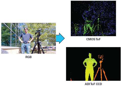
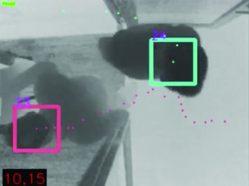
Figure 10 shows an example where three different depth measurement systems were used outdoors to measure distance. Notethat while a CMOS ToF system that used an 850nm light source has difficulty distinguishing both the person and the tripod, the ToFCCD system was able to distinguish both more clearly.
Which Applications Are Leveraging ToF Technology?
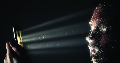
As mentioned in the introduction, the addition of depth information to a 2D image allows useful information to be extracted and can greatly improve the quality of scene information. For example, 2D sensing cannot distinguish between a real person and a photograph. Extracting depth information allows better classification of people, tracking both their facial and body features. ToF depth sensing can provide high quality and reliable face recognition for security authentication. The higher the resolution and depth accuracy, the better the classification algorithm. This can be used for simple functions such as allowing access to mobiledevices/our personal home space, or for high end use cases such as secure door access control in commercially sensitive areas.
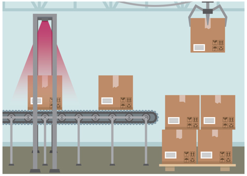
As depth sensing technologies achieve higher resolutions and depth accuracies, the classification and tracking of people will become easier. The use of artificial intelligence will allow for classification with very high confidence, which in turn will create new and emerging application areas. One use case is for a commercial automatic door opening function, especially in areas of strong sunlight. Ensuring a door only opens for a person and not anything else can provide efficiencies in building management, as well as in security and safety.

As 3D algorithms mature further, data analytics will be leveraged to gather lots of meaningful information about people’s behaviour. The first wave of this is likely to happen in building control applications such as door entry/exit systems for people-counting. The addition of depth information from a vertically mounted sensor means that people can be counted with very high accuracy. Another use case is a smart automatic door opening (Figure 13) where people can be classified and the door only opens when a real person is detected. ADI is developing software algorithms in the area of people-counting and classification.
Depth information allows high accuracy classification of people under many challenging conditions, such as environments with low or no ambient light, in areas where there is a significant density of people, and where people are well camouflaged (for example, with hats, scarves, etc.). Most importantly, the false triggering of people-counting is virtually eliminated. Today, stereo cameras can be used for entry/exit detection, but due to the limitations of mechanical size (two sensors) and high processor needs, stereo tends to be expensive and of a large form factor. As the ADI ToF technology directly outputs a depth map and only has one sensor, both the form factor and processing needs are much reduced.
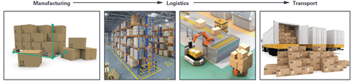
An important application of depth sensing will be in the industrial, manufacturing, and construction process. The ability to accurately dimension and classify objects in real time through a production process is not trivial. Accurate depth sensing candetermine space utilisation of warehouse bays. Products that come off a production line need to be dimensioned quickly for transfer. High resolution depth sensing will allow edges and lines of target objects to be determined in real time, and fast volume calculations made. A neural network approach is already being used in such volume determination.
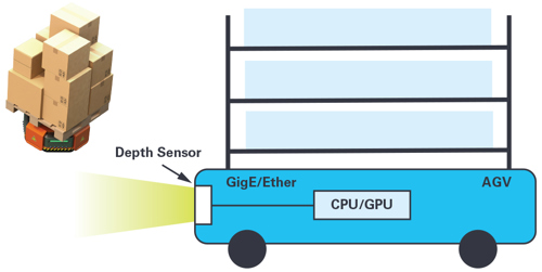
The autonomous transfer of product within a factory continues to increase. Autonomous vehicles like AGVs (autonomous guided vehicles) will need to self-navigate faster through the factory and warehouse. High accuracy depth sensing technology will allow sensors to map out their environment in real time, localise themselves within that map, and then plot the most efficient navigation path. One of the biggest challenges with the deployment of such technology in factory automation is the interference from other sensors that may operate in the same area. ADI’s interference cancellation IP will allow many such sensors to operate directly in each other’s line of sight without affecting the performance.
How Can I Evaluate, Prototype, and Design with ToF Technology?
ADI has developed an optical sensor board (AD-96TOF1-EBZ) that is compatible with the Arrow 96 application processor platform.This 96TOF1 board’s optical specifications are listed in Table 1.
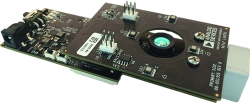
Table 1. ADI’s 96TOF Optical Board Specifications

This board can interface directly to Arrow’s 96Boards family. The 96Boards family is a range of hardware processor platforms that make the latest ARM®-based processors available to developers at a reasonable cost. Boards produced to the 96Boardsspecifications are suitable for rapid prototyping, Qualcomm® Snapdragon™, and NXP and NVIDIA® processors are all supported within the 96Boards platform.
ToF depth sensing is a complex technology. There is significant optical expertise needed to achieve the highest performance of the VGA sensor. Optical calibration, high speed pulse timing patterns, temperature drifts, and compensation will all affect depth accuracy. Design cycles can be long to achieve the desired performance. While ADI can support chip-down designs for qualified customer opportunities, many customers are looking for an easier, faster, and more efficient approach to get to market.
Many customers are interested in a simple demonstration module to first evaluate the performance of the technology, beforemoving forward with a real project. ADI has worked with various hardware partners to provide different levels of hardware offerings. The DCAM710 demonstration module, offered by one of our hardware partners (Pico) supports USB depth image streaming directly to a PC.
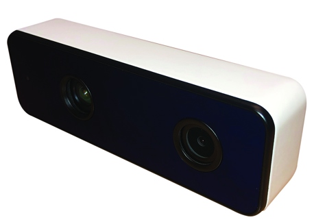
DCAM710 Module Specifications
The specifications of the ToF camera DCAM710 module are:
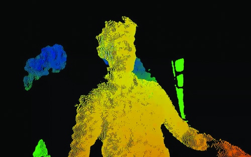
The Pico SDK software platform can support Windows and Linux operating systems and supports several software functions. Apoint cloud, which can generate a set of data points in space around an object, and which are often used to generate 3D models, is easily generated through the SDK.
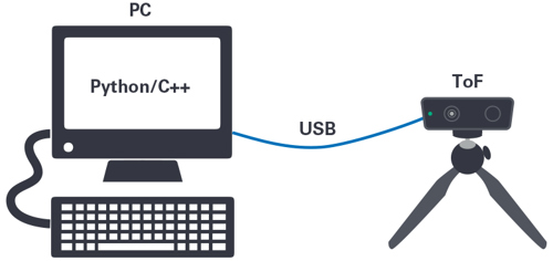
As the demonstration platform streams raw data to a computer via USB, it is easy to develop simple software application algorithms to get customers developing code quickly.
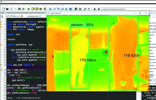
ADI provides simple sample code in Python to support customer evaluations. The example below shows a screen shot of real-time Python source code being used to detect and classify a person, and then apply a depth measurement to determine where theperson is relative to the sensor. Other algorithms that are available include edge detection, object tracking, and a 3D safety curtain.
How Do I Go to Production with ToF?
While the ADI 96TOF reference design is useful for customers doing a chip-down design and the DCAM710 demonstration platform is a cost efficient way to evaluate the technology, in many cases, customers may need a different or more customised solution when they go to production. For example, in AGV systems, a GigE or Ethernet output from an edge node sensing module is often desirable. This gives a robust method of sending high speed, raw depth data from an edge node sensing module to a centralised CPU/GPU controller.
In other applications, customers may want to implement some edge node processing and only send metadata back to the controller. In this case, having a small form factor depth node module with an integrated edge node processor supporting ARM or an FPGA is more desirable. ADI has developed a set of third-party ecosystem partners that can meet all customers’ requirements.
These third parties offer a range of capabilities, from complete camera products to small optical modules without external housing that can be integrated into bigger systems. The diagram below shows a tiny MIPI module without external housing that can easilybe mechanically integrated into bigger systems. ADI’s partner network can also offer customisation of hardware, optics, and application processors if needed. An example of the modules our partners offer today are USB, Ethernet, Wi-Fi, and MIPI, with a range of integrated edge node processors available.
Both ADI and our hardware partners also work with external software partners who bring algorithm expertise in depth processing at the application level.
Conclusion
The advantages of high resolution depth imaging to solve difficult and complex tasks in new and emerging application areas are forcing our customers to quickly drive its adoption. The fastest, lowest risk, and cheapest path to get to market is through affordable, small form factor, high precision modules that can be integrated into larger systems. ADI’s 96TOF reference design platform provides a complete embedded evaluation platform, enabling customers to immediately evaluate the technology and start developing application code. Please contact ADI for more information about ADI’s ToF technology, hardware, or our hardware partners.
Analog Devices: www.analog.com
About the Author
Colm Slattery graduated from the University of Limerick with a bachelor of electronics engineering degree. He joined ADI in 1998 and has held various roles including test development and product and system applications. Colm has also spent three years on assignment in a field role in China. Colm is currently a marketing manager in the Industrial Business Unit, focusing on new sensor technologies and new business models. He can be reached at colm.slattery@analog.com.
About the Author
Yuzo Shida is a product marketing manager for ToF products in the Healthcare, Consumer, and Industrial Group at Analog Devices. After graduating from the University of Illinois Urbana-Champaign with an EE degree in 1990, Yuzo joined ADI, where hehas been involved in the product and business development of a variety of consumer, automotive, and industrial products. He canbe reached at yuzo.shida@analog.com.


Water Sector Talent Exodus Could Cripple The Sector
Maybe if things are essential for the running of a country and we want to pay a fair price we should be running these utilities on a not for profit...