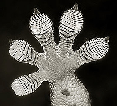
Now, a Georgia Institute of Technology (GATECH) researcher is looking into how gecko-grip could be applied in a high-precision industrial setting, such as in robot arms used in manufacturing computer chips.
"There are numerous ways that gecko adhesion could be used in an industrial setting, especially in handling delicate materials like the silicon wafers used in manufacturing computer processors," said Michael Varenberg, an assistant professor in Georgia Tech's George W Woodruff School of Mechanical Engineering.
Before robot arms and other devices can implement gecko adhesion technology, researchers need more information about the mechanical and physical characteristics of the human-made adhesive surfaces.
In a study published in Journal of the Royal Society Interface, Varenberg looked at a particular type of gecko-inspired adhesive surface and narrowed down a range of angles at which the material will attach stronger and release its grip easier.
The gecko gets its ability through the use of tiny hairs that interact with surfaces at an intermolecular level, a process during which the tiny film-like hairs are pressed onto the surface and engaged with a shearing action. They then either hold to the surface or release when pulled away in different directions.
According to GATECH, for that process to be replicated in a factory using man-made adhesive technology, researchers must determine the precise angles at which to apply a load to get or release the grip between the robotic arm and the silicon wafer.

Varenberg's team tested a wall-shaped microstructure surface moulded out of polyvinylsiloxane and designed to mimic the gecko's attachment ability. Their tests are said to have shown that the optimum attachment angle varies between 60 and 90 degrees, while the microstructures detach at zero force when the pull-off angle reaches 140-160 degrees.
"That relatively wide range to control the attachment and pulling away for these wall-shaped microstructures will make it easier to build a mechanical process around that tolerance," Varenberg said.
That could hold promise for replacing a current method used during the processing and inspection of silicon wafers in computer processor production.

Robot arms employ ceramic chucks that use vacuum or electrostatic grippers to pick up and handle the wafers. The ceramic contact posts eventually wear down due to cyclic loading and release particles that can potentially contaminate the backside of the wafer leading to lithography defects on its front side.
"This reality is inconsistent with the cleanliness standards required in the semiconductor industry," Varenberg said. "Using gecko adhesion microstructures instead would be better because they do not generate any damage to wafers and do not wear over time."
Next steps in the research include simplifying the manufacturing technique, working with industrial-grade materials as well as studying the effects of environment and surface geometry parameters, Varenberg said.


Experts speculate over cause of Iberian power outages
The EU and UK will be moving towards using Grid Forming inverters with Energy Storage that has an inherent ability to act as a source of Infinite...