The trend for making electronics and computing components smaller reaches a roadblock when it comes to some telecommunications devices. The need to carry signal means that optical fibres must be used, and these need to be long to work effectively. To avoid this problem, engineers are now using planar waveguides, which conduct light waves across a two-dimensional surface rather. Researchers at Leeds University have now developed a new way to make planar waveguides by bombarding a specific type of glass with powerful laser pulses.
The glass in question is made from compounds of zinc, sodium and tellurium, and is doped with erbium, a rare earth metal. Erbium is useful in these technologies because one of its electrons shifts orbital when it absorbs a photon of 1.5µm wavelength, a standard light wavelength used in telecommunications technologies. To make the waveguide, the researchers had to coat the glass with a thin layer of erbium, and to achieve this they fired a high-intensity laser at the surface of the doped glass. This blasted a minute crater into the material, producing a plume of ejected material that fell back to the glass surface and coated it with the metal. Using an ultrafast pulsed laser, they repeated the process many times to make a large area coating.
An important part of the research was determining the minimum energy required to separate particles in the glass surface with laser energy, known as the ablation threshold. They found that threshold does not depend on the concentration of erbium in the glass. According to Thomas Mann, an author on the paper the team published in the Journal of Applied Physics, this means the technique could be used with other dopant's that could create waveguides with different properties.
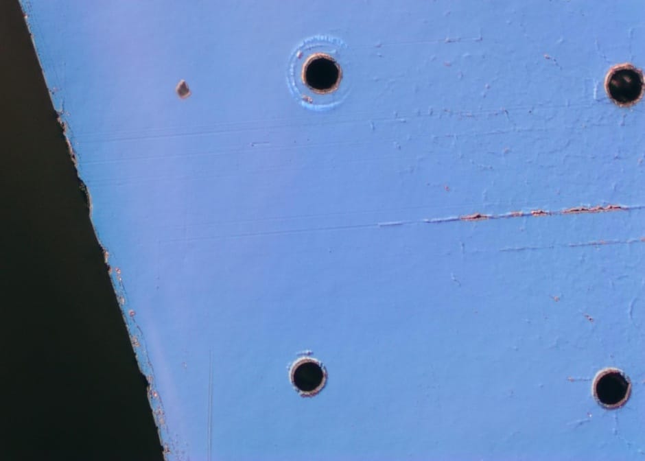
Another aspect of the study looked at the shape of the craters made by the laser blast. The paper details how the shape is important for determining the properties of the dopant coating, such as its porosity, surface area, and ability to scatter or absorb light. "These properties are important for engineering other dielectric materials for surface area-demanding applications in photocatalysis, sensing, fuel and solar cells, and light extraction in LEDs," Mann said.


McMurtry Spéirling defies gravity using fan downforce
Ground effect fans were banned from competitive motorsport from the end of the 1978 season following the introduction of Gordon Murray's Brabham...